


 The Chemical Connection: Reducing Etch System Water Usage, Part 2
 It’s Only Common Sense: Nice Guys Really Can Finish First
 The Right Approach: I Hear the Train A Comin'
Moiré Patterns of Three Layers Change the Electronic Properties of Graphene
March 11, 2019 | University of BaselEstimated reading time: 2 minutes
Combining an atomically thin graphene and a boron nitride layer at a slightly rotated angle changes their electrical properties. Physicists at the University of Basel have now shown for the first time the combination with a third layer can result in new material properties also in a three-layer sandwich of carbon and boron nitride. This significantly increases the number of potential synthetic materials, report the researchers in the scientific journal Nano Letters.
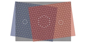
Image Caption: A graphene layer (black) of hexagonally arranged carbon atoms is placed between two layers of boron nitride atoms, which are also arranged hexagonally with a slightly different size. The overlap creates honeycomb patterns in various sizes. (Image: Swiss Nanoscience Institute, University of Basel).
Last year, researchers in the US caused a big stir when they showed that rotating two stacked graphene layers by a “magical” angle of 1.1 degrees turns graphene superconducting—a striking example of how the combination of atomically thin materials can produce completely new electrical properties.
Precision Alignment
Scientists from the Swiss Nanoscience Institute and the Department of Physics at the University of Basel have now taken this concept one step further. They placed a layer of graphene between two boron nitride layers, which is often serves to protect the sensitive carbon structure. Doing so, they aligned the layers very precisely with the crystal lattice of the graphene.
The effect observed by the physicists in Professor Christian Schönenberger’s team is commonly known as a moiré pattern: when two regular patterns are superimposed, a new pattern results with a larger periodic lattice.
New Three-Layer Superlattice
Lujun Wang, a member of the SNI PhD School and researcher in Schönenberger’s team, also observed effects of this kind of superlattice when he combined layers of boron nitride and graphene. The atoms are arranged hexagonally in all layers. If they are stacked on top of each other, larger regular patterns emerge, with a size depending on the angle between the layers.
It had already been shown that this works with a two-layer combination of graphene and boron nitride, but the effects due to a second boron nitride layer had not yet been found.
When the physicists from Basel experimented with three layers, two superlattices were formed between the graphene and the upper and the lower boron nitride layer, respectively. The superposition of all three layers created an even larger superstructure than possible with only one layer.
Scientists are very interested in these types of synthetic materials, since the different moiré patterns can be used to change or artificially produce new electronic material properties.
“To put it simply, the atomic patterns determine the behavior of electrons in a material, and we are combining different naturally occurring patterns to create new synthetic materials,” explains Dr. Andreas Baumgartner, who supervised the project. “Now we have discovered effects in these tailor-made electronic devices that are consistent with a three-layer superstructure,” he adds.
Share on:


Suggested Items
LQDX Divests Aluminum Soldering Business - Mina™ - to Taiyo America Inc.
05/02/2024 | PRNewswireLQDX, formerly known as Averatek Corp., developer of high-performance materials for advanced semiconductor manufacturing, today announced that it has divested its aluminum soldering business – known as MinaTM – to Taiyo America Inc., a global market leader in advanced electronic materials.
Indium Corporation Expert to Present on Pb-Free Solder for Die-Attach in Discrete Power Applications
04/30/2024 | Indium CorporationIndium Corporation Product Manager – Semiconductor Dean Payne will present at the Advanced Packaging for Power Electronics conference, hosted by IMAPS, held May 8-9 in Woburn, Massachusetts, USA.
Real Time with... IPC APEX EXPO 2024: Adhesive Materials and Equipment Update with Dymax
05/01/2024 | Real Time with...IPC APEX EXPOVirginia Hogan, global business development manager at Dymax, discusses adhesive materials, dispensing and curing equipment, a new, high-reliability conformal coating, and various materials and dispensing methods.
Real Time with... IPC APEX EXPO 2024: Sustainability in the Industry
04/26/2024 | Real Time with...IPC APEX EXPOGuest Editor Henry Crandall and Chris Nash of Indium Corporation discuss the company's 90th anniversary and its focus on sustainability. They focus on the benefits of sustainable materials, their compatibility, and value propositions. The conversation also highlights how Durafuse LT technology's role in reducing reflow temperatures is leading to significant cost and energy savings. Nash also touches on downstream sustainability efforts such as using recycled materials for packaging.
SMC Korea 2024 to Highlight Semiconductor Materials Trends and Innovations on Industry’s Path to $1 Trillion
04/24/2024 | SEMIWith Korea a major consumer of semiconductor materials and advanced materials a key driver of innovation on the industry’s path to $1 trillion, industry leaders and experts will gather at SMC (Strategic Materials Conference) Korea 2024 on May 29 at the Suwon Convention Center in Gyeonggi-do, South Korea to provide insights into the latest materials developments and trends. Registration is open.