


 The Chemical Connection: Onshoring PCB Production—Daunting but Certainly Possible
 Marcy’s Musings: The Legislative Outlook—Helping or Hurting?
 It’s Only Common Sense: The Phone Is Still Mightier Than the Keyboard


Nano Dimension 3D Prints Side-Mounting Tech onto PCBs
April 1, 2019 | Globe NewswireEstimated reading time: 1 minute
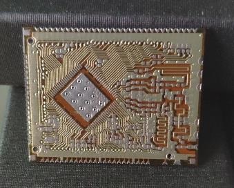
Nano Dimension Ltd. has launched the world’s first side mounting technology for additively manufactured printed circuit boards (PCBs). With Nano Dimension’s DragonFly Precision Additive Manufacturing System, the novel technology can print and solder components to the top, bottom and sides of the PCB, resulting in as much as a 50% increase in board space when compared with traditionally manufactured PCBs.
The extra space afforded through side mounting allows design engineers to pack more functionality on the circuit board, which is particularly relevant for IoT and Industry 4.0 where customized designs and shapes are a growing demand.
“For applications like the IoT where innovation is paramount, creating new electronic products in shapes and sizes that were never before possible is liberating for design engineers,” said Amit Dror, CEO of Nano Dimension. “Because of this added real estate, more functionality can be generated from sides of the board that can also be used to connect with additional boards.”
Another important enablement of side mounting is the ability to create a specialized PCB that plugs into a socket mounted on a mother board. By printing this board and inserting it into the cavity of a second board, users can rapidly customize applications based on a generic mother board.
Side mounting is ideal for applications such as modular antennas, creating non-standard packaging and innovative IoT applications. Future potential applications and benefits of Nano Dimension’s side mounting technology include printing a horizontal ground layer on the Z-axis, enabling the DragonFly Pro to produce higher performance antennas or multiple antennas with varying voltages within the board. This not only saves space but also creates limitless design possibilities.
About Nano Dimension Ltd.
Nano Dimension is a leading electronics provider that is disrupting, reshaping, and defining the future of how cognitive connected products are made. With its unique 3D printing technologies, Nano Dimension is targeting the growing demand for electronic devices that require increasingly sophisticated features. Demand for circuitry including PCBs, which are the heart of every electronic device, covers a diverse range of industries, including consumer electronics, medical devices, defense, aerospace, automotive, IoT and telecom. These sectors can all benefit greatly from Nano Dimension’s products and services for rapid prototyping and short-run manufacturing.
Share on:


Testimonial
"Advertising in PCB007 Magazine has been a great way to showcase our bare board testers to the right audience. The I-Connect007 team makes the process smooth and professional. We’re proud to be featured in such a trusted publication."
Klaus Koziol - atgSuggested Items
Rehm Wins Mexico Technology Award for CondensoXLine with Formic Acid
10/17/2025 | Rehm Thermal SystemsModern electronics manufacturing requires technologies with high reliability. By using formic acid in convection, condensation, and contact soldering, Rehm Thermal Systems’ equipment ensures reliable, void-free solder joints — even when using flux-free solder pastes.
Indium Experts to Deliver Technical Presentations at SMTA International
10/14/2025 | Indium CorporationAs one of the leading materials providers to the power electronics assembly industry, Indium Corporation experts will share their technical insight on a wide range of innovative solder solutions at SMTA International (SMTAI), to be held October 19-23 in Rosemont, Illinois.
Knocking Down the Bone Pile: Revamp Your Components with BGA Reballing
10/14/2025 | Nash Bell -- Column: Knocking Down the Bone PileBall grid array (BGA) components evolved from pin grid array (PGA) devices, carrying over many of the same electrical benefits while introducing a more compact and efficient interconnect format. Instead of discrete leads, BGAs rely on solder balls on the underside of the package to connect to the PCB. In some advanced designs, solder balls are on both the PCB and the BGA package. In stacked configurations, such as package-on-package (PoP), these solder balls also interconnect multiple packages, enabling higher functionality in a smaller footprint.
Indium to Showcase High-Reliability Solder and Flux-Cored Wire Solutions at SMTA International
10/09/2025 | Indium CorporationAs one of the leading materials providers in the electronics industry, Indium Corporation® will feature its innovative, high-reliability solder and flux-cored wire products at SMTA International (SMTAI), to be held October 19-23 in Rosemont, Illinois.
‘Create your Connections’ – Rehm at productronica 2025 in Munich
10/08/2025 | Rehm Thermal SystemsThe electronics industry is undergoing dynamic transformation: smart production lines, sustainability, artificial intelligence, and sensor technologies dominate current discussions.