


 The Chemical Connection: Reducing Etch System Water Usage, Part 2
 It’s Only Common Sense: Nice Guys Really Can Finish First
 The Right Approach: I Hear the Train A Comin'
Copper-Based Alternative for Next-Generation Electronics
April 3, 2019 | Tohoku UniversityEstimated reading time: 2 minutes
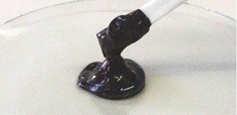
Japanese scientists have developed a technique to transform a copper-based substance into a material that mimics properties of precious and pricey metals, such as gold and silver. The new medium, made of copper nanoparticles (very small copper-based structures) has promising applications in the production of electronic devices that would otherwise depend on expensive gold and silver counterparts. It is also suitable in the fabrication of electronic components using printing technologies that are recognized as environmentally friendly production methods.
The development of the Internet of Things (IoT) has quickly increased the demand for thin and wearable electronic devices. For example, IoT depends on communication between devices, which requires antennas that have so far required expensive gold and silver-based metal composites.
To date, existing techniques for the preparation of copper nanoparticles have not been ideal as they resulted in impurities attaching to the material. Since these impurities could only be removed via extremely high temperatures, copper nanoparticles that were created at room temperature were impure and thus could not solidify into usable parts. Until now, this has been one of the hurdles to creating a more cost-effective alternative to gold and silver parts in electronic devices.The joint study between researchers at Tohoku University and Mitsui Mining & Smelting Co., Ltd in Tokyo reports the successful synthesis of copper nanoparticles with the ability of solidifying at much lower temperatures while remaining pure. The team has altered the structure of the copper nanoparticles and rendered them more stable so that they do not degrade at low temperatures.
"Copper has been an attractive alternative material in the preparation of electric circuits. The most important part of using copper is altering it so that it solidifies at low temperatures. So far, that has been difficult because copper readily interacts with the moisture in the air and degrades, which turns into unstable nanoparticles. With the methods used in this study that alter the structure of the carbon and thereby making it more stable, we have successfully overcome this instability issue," adds Kiyoshi Kanie, Ph.D., associate professor at the Institute of Multidisciplinary Research for Advanced Materials of Tohoku University.
The researchers hope to expand the application of their copper-based nanoparticles beyond just electronics. They believe that this material will be useful in other sectors as well. "Our method effectively created copper nanoparticle-based materials that can be utilized in various types of on-demand flexible and wearable devices that can be fabricated easily via printing processes at a very low cost," Kanie adds.
Share on:


Suggested Items
The Chemical Connection: Reducing Etch System Water Usage, Part 2
05/02/2024 | Don Ball -- Column: The Chemical ConnectionIn my last column, I reviewed some relatively simple ways to reduce water usage in existing etch systems: cutting down cooling coil water flow, adding chillers to replace plant water for cooling, lowering flow rate nozzles for rinses, etc. This month, I’ll continue with more ways to control water usage in your etcher. Most of these are not easily retrofittable to existing equipment but should be given serious consideration when new equipment is contemplated. With the right combination of add-ons, it is possible to bring the amount of water used in an etch system to almost zero.
Designer’s Notebook: What Designers Need to Know About Manufacturing, Part 2
04/24/2024 | Vern Solberg -- Column: Designer's NotebookThe printed circuit board (PCB) is the primary base element for providing the interconnect platform for mounting and electrically joining electronic components. When assessing PCB design complexity, first consider the component area and board area ratio. If the surface area for the component interface is restricted, it may justify adopting multilayer or multilayer sequential buildup (SBU) PCB fabrication to enable a more efficient sub-surface circuit interconnect.
Insulectro’s 'Storekeepers' Extend Their Welcome to Technology Village at IPC APEX EXPO
04/03/2024 | InsulectroInsulectro, the largest distributor of materials for use in the manufacture of PCBs and printed electronics, welcomes attendees to its TECHNOLOGY VILLAGE during this year’s IPC APEX EXPO at the Anaheim Convention Center, April 9-11, 2024.
ENNOVI Introduces a New Flexible Circuit Production Process for Low Voltage Connectivity in EV Battery Cell Contacting Systems
04/03/2024 | PRNewswireENNOVI, a mobility electrification solutions partner, introduces a more advanced and sustainable way of producing flexible circuits for low voltage signals in electric vehicle (EV) battery cell contacting systems.
Heavy Copper PCBs: Bridging the Gap Between Design and Fabrication, Part 1
04/01/2024 | Yash Sutariya, Saturn Electronics ServicesThey call me Sparky. This is due to my talent for getting shocked by a variety of voltages and because I cannot seem to keep my hands out of power control cabinets. While I do not have the time to throw the knife switch to the off position, that doesn’t stop me from sticking screwdrivers into the fuse boxes. In all honesty, I’m lucky to be alive. Fortunately, I also have a talent for building high-voltage heavy copper circuit boards. Since this is where I spend most of my time, I can guide you through some potential design for manufacturability (DFM) hazards you may encounter with heavy copper design.