


 Happy’s Tech Talk #28: The Power Mesh Architecture for PCBs
 It’s Only Common Sense: Would You Join Your Own Company?
 The Chemical Connection: Reducing Etch System Water Usage, Part 2
Unprecedented Insight Into 2D Magnets Using Diamond Quantum Sensors
April 29, 2019 | University of BaselEstimated reading time: 3 minutes
For the first time, physicists at the University of Basel have succeeded in measuring the magnetic properties of atomically thin van der Waals materials on the nanoscale. They used diamond quantum sensors to determine the strength of the magnetization of individual atomic layers of the material chromium triiodide. In addition, they found a long-sought explanation for the unusual magnetic properties of the material. The journal Science has published the findings.
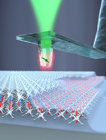
Image Caption: A diamond quantum sensor is used to determine the magnetic properties of individual atomic layers of the material chromium triiodide in a quantitative manner. It was shown that the direction of the spins in successive layers alternate in the layers. (University of Basel, Department of Physics)
The use of atomically thin, two-dimensional van der Waals materials promises innovations in numerous fields in science and technology. Scientists around the world are constantly exploring new ways to stack different single atomic layers and thus engineer new materials with unique, emerging properties.
These super-thin composite materials are held together by van der Waals forces and often behave differently to bulk crystals of the same material. Atomically thin van der Waals materials include insulators, semiconductors, superconductors and a few materials with magnetic properties. Their use in spintronics or ultra-compact magnetic memory media is highly promising.
The First Quantitative Measurement of Magnetization
Until now, it has not been possible to determine the strength, alignment and structure of these magnets quantitatively nor on the nanoscale. The team headed by Georg-H.-Endress Professor Patrick Maletinsky from the Department of Physics and the Swiss Nanoscience Institute at the University of Basel have demonstrated that the use of diamond tips decorated with single electron spins in an atomic force microscope is ideally suited to these types of studies.
“Our method, which uses the individual spins in diamond color centers as sensors, opens up a whole new field. The magnetic properties of two-dimensional materials can now be studied on the nanoscale and even in a quantitative manner. Our innovative quantum sensors are perfectly suited to this complex task,” says Maletinsky.
The Number of Layers is Critical
Using this technology which was originally developed in Basel and which is based on a single electron spin, the scientists collaborated with researchers from the University of Geneva to determine the magnetic properties of single atomic layers of chromium triiodide (CrI3). The researchers were thus able to find the answer to a key scientific question about the magnetism of this material.
As a three-dimensional, bulk crystal, chromium triiodide is fully magnetically ordered. In the case of few atomic layers, however, only stacks with an odd number of atomic layers show a non-zero magnetization. Stacks with an even number of layers exhibit an antiferromagnetic behavior; i.e. they are not magnetized. The cause of this “even/odd-effect” and the discrepancy to bulk material was previously unknown.
Strain as the Cause
Maletinsky’s team was able to demonstrate that this phenomenon is due to the specific atomic arrangement of the layers. During sample preparation, the individual chromium triiodide layers slightly move against one another. The resulting strain in the lattice means the spins of successive layers are unable to align in the same direction; instead, the spin direction alternates in the layers. With an even number of layers, the magnetization of the layers cancel out; with an odd number, the strength of the measured magnetization corresponds to that of a single layer.
However, when the strain in the stack is released—for example, by puncturing the sample—the spins of all layers can align in the same direction, as is also observed in bulk crystals. The magnetic strength of the entire stack is then consistent with the sum of the individual layers.
The work conducted by the Basel scientists thereby not only answers a key question about two-dimensional van der Waals magnets, it also opens interesting perspectives on how their innovative quantum sensors can be used in the future to study two-dimensional magnets in order to contribute to the development of novel electronic components.
Share on:


Suggested Items
2024 Apple iPad Pro Estimated to Ship Between 4.5 to 5 Million Units
05/08/2024 | TrendForceApple’s recent product launch in May introduced a lineup of new tablets featuring advanced AMOLED screens. Notably, the Pro version boasts a dual-layer tandem structure designed to address the longstanding challenges of screen burn-in and lifespan that are common with AMOLED displays.
AIM Solder Signs Shinil Fl Ltd. as New Distributor for Korea
05/08/2024 | AIM SolderAIM Solder, a leading global manufacturer of solder assembly materials for the electronics industry, is pleased to announce a new distribution partnership with Shinil Fl Ltd., a prominent supplier of technological solutions in the SMT and semiconductor sectors.
IDTechEx Discusses Low-Loss Materials: The Enabler of Future Connected Vehicles?
05/06/2024 | IDTechExFuture connected vehicles will offer future drivers a safer, smoother, and more convenient driving experience. Not only will drivers get access to more navigation and entertainment options, but they will also gain access to safety technologies that will potentially reduce accidents, improve congestion, and reduce emissions globally by allowing vehicle safety systems to communicate with each other and with city traffic infrastructure.
LQDX Divests Aluminum Soldering Business - Mina™ - to Taiyo America Inc.
05/02/2024 | PRNewswireLQDX, formerly known as Averatek Corp., developer of high-performance materials for advanced semiconductor manufacturing, today announced that it has divested its aluminum soldering business – known as MinaTM – to Taiyo America Inc., a global market leader in advanced electronic materials.
Indium Corporation Expert to Present on Pb-Free Solder for Die-Attach in Discrete Power Applications
04/30/2024 | Indium CorporationIndium Corporation Product Manager – Semiconductor Dean Payne will present at the Advanced Packaging for Power Electronics conference, hosted by IMAPS, held May 8-9 in Woburn, Massachusetts, USA.