


 The Chemical Connection: Reducing Etch System Water Usage, Part 2
 It’s Only Common Sense: Nice Guys Really Can Finish First
 The Right Approach: I Hear the Train A Comin'
New Topological Insulator Can Reroute Photonic ‘Traffic’ On the Fly, Making for Faster Chips
September 16, 2019 | PennEngineeringEstimated reading time: 3 minutes
Topological insulators are a game-changing class of materials; charged particles can flow freely on their edges and route themselves around defects, but can’t pass through their interiors. This perfect surface conduction holds promise for fast and efficient electronic circuits, though engineers must contend with the fact that the interiors of such materials are effectively wasted space.
Now, researchers from the University of Pennsylvania, where topological insulators were first discovered in 2005, have shown a way to fulfill that promise in a field where physical space is at an even bigger premium: photonics. They have shown, for the first time, a way for a topological insulator to make use of its entire footprint.
By using photons instead of electrons, photonic chips promise even faster data transfer speeds and information-dense applications, but the components necessary for building them remain considerably larger than their electronic counterparts, due to the lack of efficient data-routing architecture.
A photonic topological insulator with edges that can be redefined on the fly, however, would help solve the footprint problem. Being able to route these “roads” around one another as needed means the entire interior bulk could be used to efficiently build data links.
Researchers at Penn’s School of Engineering and Applied Science have built and tested such a device for the first time, publishing their findings in the journal Science.
“This could have a big impact on large-information capacity applications, like 5G, or even 6G, cellphone networks,” says Liang Feng, assistant professor in Penn Engineering’s Departments of Materials Science and Engineering and Electrical and Systems Engineering.
“We think this may be the first practical application of topological insulators,” he says.
Feng led the study along with graduate student Han Zhao, a member of his lab. Fellow lab members Xingdu Qiao, Tianwei Wu and Bikashkali Midya, along with Stefano Longhi, professor at the Polytechnic University of Milan in Italy, also contributed to the research.
The data centers that form the backbone of communication networks route calls, texts, email attachments and streaming movies to and between millions of cellular devices. But as the amount of data flowing through these data centers increases, so does the need for high-capacity data routing that can keep up with the demand.
Switching from electrons to photons would speed up this process for the upcoming information explosion, but engineers must first design a whole new library of devices for getting those photons from input to output without mixing them up and losing them in the process.
Advances in data-processing speed in electronics have relied on making their core components smaller and smaller, but photonics researchers have needed to take a different approach.
Feng, Zhao and their colleagues set out to maximize the complexity of photonic waveguides — the prescribed paths individual photons take on their way from input to output — on a given chip.
Microscope details of the researchers’ photonic chip
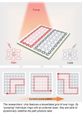
The researchers’ prototype photonic chip is roughly 250 microns squared, and features a tessellated grid of oval rings. By “pumping” the chip with an external laser, targeted to alter the photonic properties of individual rings, they are able to alter which of those rings constitute the boundaries of a waveguide.
The result is a reconfigurable topological insulator. By changing the pumping patterns, photons headed in different directions can be routed around each other, allowing photons from multiple data packets to travel through the chip simultaneously, like a complicated highway interchange.
“We can define the edges such that photons can go from any input port to any output port, or even to multiple outputs at once,” Feng says. “That means the ports-to-footprint ratio is at least two orders of magnitude greater than current state-of-the-art photonic routers and switches.”
Increased efficiency and speed is not the only advantage of the researchers’ approach.
“Our system is also robust against unexpected defects,” Zhao says. “If one of the rings is damaged by a grain of dust, for example, that damage is just making a new set of edges that we can send photons along.”
Since the system requires an off-chip laser source to redefine the shape of the waveguides, the researcher’s system is not yet small enough to be useful for data centers or other commercial applications. Next steps for the team will be to establish a fast reconfiguring scheme in an integrated fashion.
Share on:


Suggested Items
Industrial PC Market Size to Record $1.75 Billion Growth from 2023-2027
05/03/2024 | PRNewswireThe global industrial pc market size is estimated to grow by USD 1.75 billion from 2023 to 2027, according to Technavio. This growth is expected to occur at a Compound Annual Growth Rate (CAGR) of almost 6.29% during the forecast period.
Gartner Survey Finds 61% of Organizations Are Evolving Their D&A Operating Model Because of AI Technologies
05/01/2024 | Gartner, Inc.Sixty-one percent of organizations are forced to evolve or rethink their data and analytics (D&A) operating model because of the impact of disruptive artificial intelligence (AI) technologies, according to a new Gartner, Inc. survey.
Real Time with… IPC APEX EXPO 2024: Operational Excellence and Smart Factory Initiatives
04/30/2024 | Real Time with...IPC APEX EXPOOperational excellence and operational efficiency are defined in this interview with Koh Young General Manager Joel Scutchfield. He touches on automation, AI, and collaboration as solutions to resource limitations. Koh Young's data-driven approach uses AI for process adjustments, data analytics, and supply chain enhancements. The discussion underscores the shift toward smart factory initiatives and the future of manufacturing, with a focus on reshoring, nearshoring, and technology utilization.
IDTechEx Report on Quantum Technology: Nano-scale Physics for Massive Market Impact
04/30/2024 | PRNewswireThe quantum technology market leverages nano-scale physics to create revolutionary new devices for computing, sensing, and communications. Across the industry, quantum technology offers a paradigm shift in performance compared with incumbent solutions.
NASA’s Optical Comms Demo Transmits Data Over 140 Million Miles
04/30/2024 | NASA JPLNASA’s Deep Space Optical Communications experiment also interfaced with the Psyche spacecraft’s communication system for the first time, transmitting engineering data to Earth.