


 Marcy’s Musings: The Legislative Outlook—Helping or Hurting?
 It’s Only Common Sense: The Phone Is Still Mightier Than the Keyboard
 The Marketing Minute: Marketing With Layers


Toray Creates Revolutionary PPS Film for 5G Circuit Boards
December 23, 2019 | Toray IndustriesEstimated reading time: 2 minutes
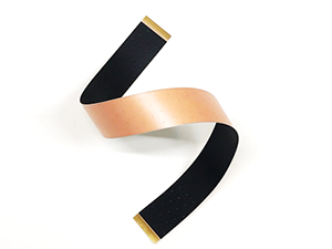
Toray Industries, Inc., announced that it has created a polyphenylene sulfide (PPS) film that maintains the outstanding dielectric characteristics—or low dielectric losses of electrical energy—flame retardancy, and chemical robustness of that polymer while remaining thermally resistant at 40°C higher than conventional counterparts. The new film resists deformation and is dimensionally stable near its melting point. PPS is a super engineering plastic that also offers excellent electrical insulation. It is crystalline, with a melting point of 280°C.
Employing the new film in flexible printed circuits offering 5G and other fast data rates would offer two key benefits. First, the film would cut the transmission losses of communication devices at high frequencies. Second, it would help stabilize high-speed communication across the temperature and humidity spectrums. Flexible printed circuits are film-like wiring boards in which electrical circuits are formed on base materials from bonding thin, soft insulating base films with copper foil or other conductive metals.
Toray has already completed the technology for the new film on a pilot basis, and looks to have a mass production setup in place during fiscal 2020 that would help swiftly popularize devices in the fast-expanding 5G arena. 5G is commanding attention as an advanced platform for delivering outstanding speed capacity, multi-connectivity, and low latency. It harnesses frequency bands below 6 GHz and above 20 GHz.
Development efforts have seen the emergence of practical liquid crystal polymer (LCP) films as flexible printed circuit substrate materials needed for 5G. The dielectric properties of such films reduce transmission losses in high-frequency bands. These films also offer thermal resistance when soldering circuit boards. The expense and processing issues of LCP films fueled the exploration of other materials that could overcome those shortcomings.
Generally PPS film offers superior flame retardancy and chemical resistance while matching or exceeding the dielectric properties of LCP film, and is far less vulnerable to temperature and humidity extremes. On the downside, PPS film deforms easily at high temperatures and provides insufficient resistance to heat when soldering circuit boards.
These considerations drove Toray to blaze a new trail in film design. It was in the course of that effort that it developed a proprietary technology that controls the crystal structure of PPS films. It thereby maintained the outstanding properties of PPS polymer while dramatically increasing thermal resistance.
Testing to 250°C confirmed that Toray’s new PPS film does not deform. Increasing thermal resistance should make it possible to employ existing processing facilities of circuit boards. Toray attained a low coefficient of thermal expansion in the thickness direction of 98 ppm/°C by employing technology it has amassed over many years to control the orientation of film molecular chains. The diverse applications that leveraging those features, including 5G transmission cables and antennas, should enable the design of smaller, multi-layered circuit boards.
By taking advantage of the high thermal dimensional stability and cost-competitiveness of TORELINA, its biaxially-oriented PPS film, Toray looks to secure the adoption of its new film in the FPC market, particularly for smartphones, and thereafter cultivate diverse applications, including for vehicular usage and base stations. In so doing, the company will create new value in keeping with its corporate philosophy of contributing to society through innovative ideas, technologies, and products.
Share on:


Testimonial
"Advertising in PCB007 Magazine has been a great way to showcase our bare board testers to the right audience. The I-Connect007 team makes the process smooth and professional. We’re proud to be featured in such a trusted publication."
Klaus Koziol - atgSuggested Items
Episode 6 of Ultra HDI Podcast Series Explores Copper-filled Microvias in Advanced PCB Design and Fabrication
10/15/2025 | I-Connect007I-Connect007 has released Episode 6 of its acclaimed On the Line with... American Standard Circuits: Ultra High Density Interconnect (UHDI) podcast series. In this episode, “Copper Filling of Vias,” host Nolan Johnson once again welcomes John Johnson, Director of Quality and Advanced Technology at American Standard Circuits, for a deep dive into the pros and cons of copper plating microvias—from both the fabricator’s and designer’s perspectives.
Nolan’s Notes: Tariffs, Technologies, and Optimization
10/01/2025 | Nolan Johnson -- Column: Nolan's NotesLast month, SMT007 Magazine spotlighted India, and boy, did we pick a good time to do so. Tariff and trade news involving India was breaking like a storm surge. The U.S. tariffs shifted India from one of the most favorable trade agreements to the least favorable. Electronics continue to be exempt for the time being, but lest you think that we’re free and clear because we manufacture electronics, steel and aluminum are specifically called out at the 50% tariff levels.
MacDermid Alpha & Graphic PLC Lead UK’s First Horizontal Electroless Copper Installation
09/30/2025 | MacDermid Alpha & Graphic PLCMacDermid Alpha Electronics Solutions, a leading supplier of integrated materials and chemistries to the electronics industry, is proud to support Graphic PLC, a Somacis company, with the installation of the first horizontal electroless copper metallization process in the UK.
Electrodeposited Copper Foils Market to Grow by $11.7 Billion Over 2025-2032
09/18/2025 | Globe NewswireThe global electrodeposited copper foils market is poised for dynamic growth, driven by the rising adoption in advanced electronics and renewable energy storage solutions.
MacDermid Alpha Showcases Advanced Interconnect Solutions at PCIM Asia 2025
09/18/2025 | MacDermid Alpha Electronics SolutionsMacDermid Alpha Electronic Solutions, a global leader in materials for power electronics and semiconductor assembly, will showcase its latest interconnect innovations in electronic interconnect materials at PCIM Asia 2025, held from September 24 to 26 at the Shanghai New International Expo Centre, Booth N5-E30