-
- News
- Books
Featured Books
- pcb007 Magazine
Latest Issues
Current IssueAdvancing the Advanced Materials Discussion
Moore’s Law is no more, and the advanced material solutions to grapple with this reality are surprising, stunning, and perhaps a bit daunting. Buckle up for a dive into advanced materials and a glimpse into the next chapters of electronics manufacturing.
Inventing the Future With SEL
Two years after launching its state-of-the-art PCB facility, SEL shares lessons in vision, execution, and innovation, plus insights from industry icons and technology leaders shaping the future of PCB fabrication.
Sales: From Pitch to PO
From the first cold call to finally receiving that first purchase order, the July PCB007 Magazine breaks down some critical parts of the sales stack. To up your sales game, read on!
- Articles
- Columns
- Links
- Media kit
||| MENU - pcb007 Magazine
Is Glass Finally Coming of Age?
October 13, 2025 | Nolan Johnson, I-Connect007Estimated reading time: 1 minute

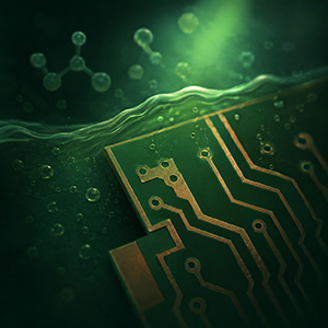
Substrates, by definition, form the base of all electronic devices. Whether discussing silicon wafers for semiconductors, glass-and-epoxy materials in printed circuits, or the base of choice for interposers, all these materials function as substrates.
While other substrates have come and gone (polyimide paper, unreinforced PTFE, epoxied paper, and Bakelite for printed circuits, and germanium, selenium, and gallium arsenide for semiconductors), silicon (for semiconductors), and FR-4 (for printed circuits) have remained the de facto standards for the industry. These represent the majority of substrates in use over the past 25 years or more.
The industry seemed content with these substrate choices as long as Moore's Law held. But now, after years of relative stability in substrates across all aspects of the electronics industry, multiple simultaneous advances in materials are breaking through.
Moore’s Law No More, Now What?
With Moore’s Law having reached its practical limits in monolithic silicon, new approaches (heterogeneous integration, advanced packaging) and new substrate materials are in demand to keep the miniaturization momentum. For both semiconductors and PCBs (or interconnects), glass is one contender that may be far less complex than some of its predecessors.
Planarity is a key advantage of glass. Glass delivers such extreme planarity because, as an amorphous material, it has no underlying weave like FR-4. The glass fiber weave comes with localized unevenness and a tendency to deform under heat—traits that become even more apparent on traditional substrate materials as PCB feature sizes get significantly smaller and larger.
To continue reading this article, which originally appeared in the September 2025 issue of PCB007 Magazine, click here.
Testimonial
"Advertising in PCB007 Magazine has been a great way to showcase our bare board testers to the right audience. The I-Connect007 team makes the process smooth and professional. We’re proud to be featured in such a trusted publication."
Klaus Koziol - atgSuggested Items
The Chemical Connection: Experience and Wisdom Gained by Doing Business
09/03/2025 | Don Ball -- Column: The Chemical ConnectionA well-managed company learns to adjust its strategies and processes based on what it learns during challenging times. The experience gained from making (or losing) a difficult sale is invaluable in adapting new sales and manufacturing processes necessary to make that sale the next time, no matter how painful those new processes might be.
Materials and Manufacturing for the AI Era: The Next PCB Frontier
08/08/2025 | Edy Yu, Chief Editor, ECIO, and the I-Connect007 Editorial TeamAI is pushing hardware to its limits, and the bottleneck isn’t design anymore—it’s materials. Next-generation AI servers aren’t just heavier on layer counts. They demand better materials to handle the speed, heat, and signal integrity requirements of 400G, 800G, and even 1.6T Ethernet systems. Many server motherboards are already 32–36 layers. For the next wave of 1.6T-capable boards, expect 40–50 layers, which must maintain high-frequency performance without degrading signal quality.
I-Connect007 Editor’s Choice: Five Must-Reads for the Week
06/27/2025 | Nolan Johnson, I-Connect007While news outside our industry keeps our attention occupied, the big news inside the industry is the rechristening of IPC as the Global Electronics Association. My must-reads begins with Marcy LaRont’s exclusive and informative interview with Dr. John Mitchell, president and CEO of the Global Electronics Association. For designers, have we finally reached the point in time where autorouters will fulfill their potential?
The Chemical Connection: Through-glass Vias in Glass Substrates
06/24/2025 | Don Ball -- Column: The Chemical ConnectionThis month’s theme is vias and how best to ensure via quality and reliability. I don’t have much expertise in this process area or much to contribute that most of you don’t already know. However, I’ve recently become peripherally involved in a via technology that may be of more than academic interest to some of us. It entails putting vias in a material not usually associated with PCB manufacturing: through-glass vias (TGVs) in glass substrates.
Trouble in Your Tank: Causes of Plating Voids, Pre-electroless Copper
05/09/2025 | Michael Carano -- Column: Trouble in Your TankIn the business of printed circuit fabrication, yield-reducing and costly defects can easily catch even the most seasoned engineers and production personnel off guard. In this month’s column, I’ll investigate copper plating voids with their genesis in the pre-plating process steps.