


 The Marketing Minute: Marketing With Layers
 The Right Approach: Electro-Tek—A Williams Family Legacy, Part 1
 It’s Only Common Sense: If You’re Not Differentiated, You’re Dead


Toyochem Develops Highly Flexible EMI Shielding Film for High-speed FPCs
January 22, 2020 | ToyochemEstimated reading time: 1 minute
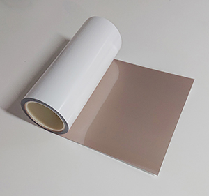
Toyochem Co., Ltd., a member of the Toyo Ink Group, has launched a highly flexible electromagnetic interference (EMI) shielding film, the LIOELM™ TSS510-HF, designed to meet the demanding performance requirements of 5G flexible printed circuits (FPCs). The newly developed TSS510-HF addresses the needs of today’s electronics designers for improved shielding performance for the transmission of high-frequency signals and for high flexibility so circuits do not break when bent.
The flexibility of FPCs has seen their adoption in a wide range of industrial and consumer electronic devices. As the mobile world transitions from 4G to 5G, the demand for higher performance flex circuits is expected to grow in line with demand for more advanced smartphones and 5G/IoT devices, including camera flex circuits, display flex circuits and wearable devices. While copper plating technology is typically used in the manufacturing of FPCs to absorb radio and other EMI waves, copper is not ideal for applications that require high flexibility, often cracking when the circuit is bent or folded, or burring during the die-cutting process.

Addressing these challenges, Toyochem technicians in Japan engineered the TSS510-HF shielding film to exhibit extraordinary flexibility, with no cracking even after bending the film 20 times at a 180 degree angle, 2kg load (see Image 2). Toyochem was able to achieve these advances by using a flexible and conductive urethane resin in place of traditional copper wiring as the EMI shielding material. The resin was first dispersed with a conductive filler, which generates a resin composite with enhanced compatibility between film flexibility and tensile strength. The optimized film structure enabled the company to solve the cracking and burring issues associated with copper foil shields.
Performance tests of the TSS510-HF shielding film demonstrated reduced transmission loss at the -6.5 dB level at 15 GHz, relative to -8.5 dB for conventional shielding films. Shielding effect testing generated values greater than 70 dB at 15 GHz, compared to 60 dB for conventional types, thereby making the TSS510-HF suitable for use in FPCs in the high-frequency band. Moreover, its exceptional bendibility offers FPC design engineers unlimited freedom in the shaping of flexible electronic devices.
Evaluation samples of LIOELM TSS510-HF are now available. The TSS510-HF and other advanced electronic solutions from Toyochem will be showcased at DesignCon 2020 from January 28 to 30, in Santa Clara, CA, USA.
Share on:


Testimonial
"We’re proud to call I-Connect007 a trusted partner. Their innovative approach and industry insight made our podcast collaboration a success by connecting us with the right audience and delivering real results."
Julia McCaffrey - NCAB GroupSuggested Items
Episode 6 of Ultra HDI Podcast Series Explores Copper-filled Microvias in Advanced PCB Design and Fabrication
10/15/2025 | I-Connect007I-Connect007 has released Episode 6 of its acclaimed On the Line with... American Standard Circuits: Ultra High Density Interconnect (UHDI) podcast series. In this episode, “Copper Filling of Vias,” host Nolan Johnson once again welcomes John Johnson, Director of Quality and Advanced Technology at American Standard Circuits, for a deep dive into the pros and cons of copper plating microvias—from both the fabricator’s and designer’s perspectives.
Nolan’s Notes: Tariffs, Technologies, and Optimization
10/01/2025 | Nolan Johnson -- Column: Nolan's NotesLast month, SMT007 Magazine spotlighted India, and boy, did we pick a good time to do so. Tariff and trade news involving India was breaking like a storm surge. The U.S. tariffs shifted India from one of the most favorable trade agreements to the least favorable. Electronics continue to be exempt for the time being, but lest you think that we’re free and clear because we manufacture electronics, steel and aluminum are specifically called out at the 50% tariff levels.
MacDermid Alpha & Graphic PLC Lead UK’s First Horizontal Electroless Copper Installation
09/30/2025 | MacDermid Alpha & Graphic PLCMacDermid Alpha Electronics Solutions, a leading supplier of integrated materials and chemistries to the electronics industry, is proud to support Graphic PLC, a Somacis company, with the installation of the first horizontal electroless copper metallization process in the UK.
Electrodeposited Copper Foils Market to Grow by $11.7 Billion Over 2025-2032
09/18/2025 | Globe NewswireThe global electrodeposited copper foils market is poised for dynamic growth, driven by the rising adoption in advanced electronics and renewable energy storage solutions.
MacDermid Alpha Showcases Advanced Interconnect Solutions at PCIM Asia 2025
09/18/2025 | MacDermid Alpha Electronics SolutionsMacDermid Alpha Electronic Solutions, a global leader in materials for power electronics and semiconductor assembly, will showcase its latest interconnect innovations in electronic interconnect materials at PCIM Asia 2025, held from September 24 to 26 at the Shanghai New International Expo Centre, Booth N5-E30