


 Dan’s Biz Bookshelf: ‘Abundance: How We Build a Better Future’
 Trouble in Your Tank: In Complex Systems, Design Rules Aren’t Optional
 It’s Only Common Sense: The Phone Is Still Your Competitive Advantage


JEOL Introduces New Field Emission SEM With Automated Analytical Intelligence
January 29, 2020 | JEOL USAEstimated reading time: 2 minutes
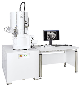
JEOL introduces a new Field Emission Scanning Electron Microscope with several features unique to the company’s FE SEM product line: NeoEngine, employing analytical intelligence for optimizing electron beam setup and tuning; embedded EDS with Live Analysis for real time imaging and elemental analysis; and Zeromag navigation function, seamlessly transitioning between optical imaging to nanoscale investigation with the high-powered optics of the SEM.
"JEOL’s F100 FE-SEM offers a truly revolutionary approach to address users’ high-resolution microscopy and microanalysis needs. In a single platform JEOL combined the best electron optics with fully embedded EDS microanalysis and the powerful AI algorithms of NeoEngine to achieve the ultimate ease of use and streamlined workflow," says Dr. Natasha Erdman, FESEM Product Manager.
NeoEngine corrects electron trajectories and automatically aligns the beam in real time, plus automatically corrects focus, brightness/contrast, and astigmatism. The SEM achieves single-digit Angstrom resolution at low kV, ideal for ultrahigh high-resolution imaging of nanostructures, specimen surface details, biological specimens, and magnetic samples as well as elemental analysis of non-conductive and beam sensitive samples.
Fully embedded EDS with Live Analysis allows the user to simply select the area, mapping, line, or another type of analysis directly on the observation screen to begin automatic live display of the elements in the specified location.
The large specimen chamber of the JSM-F100 features multiple ports for analytical applications: EDS, WDS, EBSD, STEM, BSE, and CL. An optional Soft X-ray Emission Spectrometer provides efficient and parallel collection of very low-energy X-rays while providing unprecedented chemical state analysis.
The JEOL JSM-F100 features an in-lens detector and energy filter, an Aperture Angle Control Lens (ACL) for superb resolution at any kV or probe current, Beam Deceleration (BD) mode for charge reduction and enhanced surface detail, and a variable pressure option for non-conductive specimens.
Never before has the power of Field Emission SEM been so easy to use. With the introduction of JEOL’s next-generation streamlined FE SEM product line, operator controls are simplified and the functions of the SEM fully automated for optimum performance. Imaging and analysis data are quickly obtained and reported through the effortless data management system.
Share on:


Subscribe
Stay ahead of the technologies shaping the future of electronics with our latest newsletter, Advanced Electronics Packaging Digest. Get expert insights on advanced packaging, materials, and system-level innovation, delivered straight to your inbox.
Subscribe now to stay informed, competitive, and connected.
Suggested Items
Gregoire Outters Promoted to President of Teledyne Marine Group
04/06/2026 | TeledyneTeledyne Technologies Incorporated announced the promotion of Gregoire Outters to President of its Teledyne Marine Group.
Teledyne Strengthens Commitment to the Space Sector
04/01/2026 | BUSINESS WIRETeledyne Technologies Incorporated is excited to announce the integration of the company’s extensive portfolio of space-focused technologies and businesses, reinforcing its long-term commitment to the global space sector.
Teledyne to Supply Detectors for Lazuli Space Observatory
03/30/2026 | BUSINESS WIRETeledyne Space Imaging, part of Teledyne Technologies Incorporated has been awarded a contract by Schmidt Sciences to deliver advanced near-infrared (NIR) H4RG-10 flight focal plane arrays (FPAs) and custom electronics for integration into the Integral Field Spectrograph on the groundbreaking Lazuli Space Observatory.
New Superconducting Chip Could Enable Breakthrough Nondestructive Terahertz Imaging
03/23/2026 | University of GlasgowA tiny crystal chip which uses terahertz radiation to see clearly through a wide range of materials could find applications in healthcare, biological research, and security screening.
The Test Connection Adds Creative Electron Prime TruVision™ X-ray and CT System for Deeper Failure Analysis
03/05/2026 | TTCIThe Test Connection Inc. (TTCI), a trusted provider of electronic test and manufacturing solutions for more than 45 years, has added the Prime TruVision™ X-ray and computed tomography (CT) inspection system from Creative Electron to its engineering and analysis services.