


 The Chemical Connection: Reducing Etch System Water Usage, Part 2
 It’s Only Common Sense: Nice Guys Really Can Finish First
 The Right Approach: I Hear the Train A Comin'
StratEdge Features Semiconductor Packages and Assembly Services at Three Trade Shows in March
February 25, 2020 | StratEdgeEstimated reading time: 1 minute
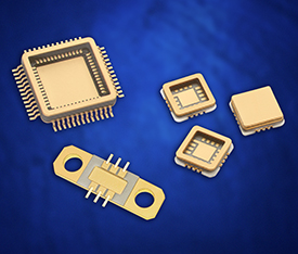
StratEdge Corporation, leader in the design, production, and assembly of high-frequency and high-power semiconductor packages for microwave, millimeter-wave, and high-speed digital devices, will have applications specialists available at the IMAPS Device Packaging Conference, APEC 2020, and GOMACTech 2020 to discuss the many packages available for DC to 63+ GHz and its package assembly services.
Packages include:
- Post-fired ceramic, low-cost molded ceramic, and ceramic QFN packages
- The LL family of leaded laminate copper-moly-copper (CMC) base packages
- High-power semiconductor packages
- Off-the-shelf molded ceramic packages that can be configured to meet the requirements for chips with frequencies up to 18 GHz. These packages provide enhanced thermal dissipation for high-power gallium nitride devices and come in fully hermetic versions in over 200 standard outlines.
- High-reliability packages that meet stringent military applications. The packages have electrical transition designs that ensure exceptionally low electrical losses and operate efficiently, even at the highest frequencies.
"Much attention is given to GaN chips, but the package in which the GaN device is attached and the way the chip is attached to the package is often overlooked," explained Casey Krawiec, VP of global sales for StratEdge Corporation. "It's well known that GaN chip efficiency and reliability can be improved by creating a package environment that reduces chip-to-package junction temperatures. StratEdge has developed a proprietary eutectic die attach method that drops junction temperatures by 20 degrees when compared to standard assembly methods with ceramic packages. Please stop by our booths and find out more."
StratEdge will be at IMAPS Device Packaging Conference, Fountain Hills, AZ, from March 3-4 in booth 56, APEC 2020, New Orleans, LA, from March 16-18 in booth 2157, and at GOMACTech 2020, San Diego, CA, from March 17-18, in booth 202.
Share on:


Suggested Items
The Chemical Connection: Reducing Etch System Water Usage, Part 2
05/02/2024 | Don Ball -- Column: The Chemical ConnectionIn my last column, I reviewed some relatively simple ways to reduce water usage in existing etch systems: cutting down cooling coil water flow, adding chillers to replace plant water for cooling, lowering flow rate nozzles for rinses, etc. This month, I’ll continue with more ways to control water usage in your etcher. Most of these are not easily retrofittable to existing equipment but should be given serious consideration when new equipment is contemplated. With the right combination of add-ons, it is possible to bring the amount of water used in an etch system to almost zero.
Designer’s Notebook: What Designers Need to Know About Manufacturing, Part 2
04/24/2024 | Vern Solberg -- Column: Designer's NotebookThe printed circuit board (PCB) is the primary base element for providing the interconnect platform for mounting and electrically joining electronic components. When assessing PCB design complexity, first consider the component area and board area ratio. If the surface area for the component interface is restricted, it may justify adopting multilayer or multilayer sequential buildup (SBU) PCB fabrication to enable a more efficient sub-surface circuit interconnect.
Insulectro’s 'Storekeepers' Extend Their Welcome to Technology Village at IPC APEX EXPO
04/03/2024 | InsulectroInsulectro, the largest distributor of materials for use in the manufacture of PCBs and printed electronics, welcomes attendees to its TECHNOLOGY VILLAGE during this year’s IPC APEX EXPO at the Anaheim Convention Center, April 9-11, 2024.
ENNOVI Introduces a New Flexible Circuit Production Process for Low Voltage Connectivity in EV Battery Cell Contacting Systems
04/03/2024 | PRNewswireENNOVI, a mobility electrification solutions partner, introduces a more advanced and sustainable way of producing flexible circuits for low voltage signals in electric vehicle (EV) battery cell contacting systems.
Heavy Copper PCBs: Bridging the Gap Between Design and Fabrication, Part 1
04/01/2024 | Yash Sutariya, Saturn Electronics ServicesThey call me Sparky. This is due to my talent for getting shocked by a variety of voltages and because I cannot seem to keep my hands out of power control cabinets. While I do not have the time to throw the knife switch to the off position, that doesn’t stop me from sticking screwdrivers into the fuse boxes. In all honesty, I’m lucky to be alive. Fortunately, I also have a talent for building high-voltage heavy copper circuit boards. Since this is where I spend most of my time, I can guide you through some potential design for manufacturability (DFM) hazards you may encounter with heavy copper design.