


 The Chemical Connection: Onshoring PCB Production—Daunting but Certainly Possible
 It’s Only Common Sense: The Phone Is Still Mightier Than the Keyboard


New Optical System Could Lead to Devices That Can Recognize Objects Instantly
March 9, 2020 | UCLA NewsroomEstimated reading time: 2 minutes
A technology developed at the UCLA Samueli School of Engineering could one day make it possible to produce optical devices that can instantaneously recognize objects without additional computer processing. The technology could ultimately be useful for robots, autonomous vehicles and other applications.
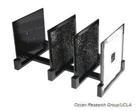
The UCLA researchers developed an optical neural network, a “maze” for beams of light, with a series of specially designed translucent wafers made of different materials such as plastic or glass. The wafers have rough surfaces — similar to frosted glass — which are designed at a scale smaller than the wavelength of light to split up light beams into various directions as they travel through the maze.
The research is described in a study published in Light: Science & Applications.
Because of how the light interacts with the wafers, each sub-band of light exiting the maze is precisely directed to a desired spot on a screen at the end of the array. That’s possible because the device can simultaneously process many wavelengths of light, in contrast to previous similar devices, also created by UCLA engineers, that could only use a single wavelength. Those earlier devices were able to identify handwritten numbers and clothing items, which are commonly used in tests of artificial intelligence systems.
“The advance is like the transition from black-and-white TV to color TV,” said Aydogan Ozcan, who led the study and is a UCLA chancellor’s professor of electrical and computer engineering. “There is richer information when you can see colors through different wavelengths of light. Most scenes naturally contain information in vivid color, so the more wavelengths that a network can ‘see,’ the more it increases the amount of information it can process.”
The beam of light that the engineers directed into the maze was composed of many wavelengths in the terahertz part of the light spectrum.
“One of the goals of this research is to create a technology that intuitively combines the capabilities of our eyes and brains, and this new study is a step toward that,” said Ozcan, who also is the associate director of the California NanoSystems Institute at UCLA. “Ultimately, we want to expand the technical capabilities of optical computation and design beyond that of human capabilities.”
The network was designed using a branch of artificial intelligence called deep learning, in which computer programs “learn” and adjust their responses accordingly based on numerous repetitions of an action or experiment.
“Traditionally, researchers use their own knowledge of physics and intuition to design optical mazes that harness and engineer light in unique ways,” Ozcan said. “Now, deep learning is surprising us in finding new methods — ones that we would normally not come up with — to solve these puzzles. It’s helping us design new optical devices that provide powerful and elegant solutions to challenging problems.”
The study’s other authors are graduate students Yi Luo, Deniz Mengu and Muhammed Veli; postdoctoral researcher Nezih Yardimci; adjunct professor Yair Rivenson; and professor Mona Jarrahi — all of whom are members of UCLA’s electrical and computer engineering department.
The study was supported in part by Fujikura, a Japanese electronics equipment manufacturer. News from Matthew Chin.
Share on:


Testimonial
"The I-Connect007 team is outstanding—kind, responsive, and a true marketing partner. Their design team created fresh, eye-catching ads, and their editorial support polished our content to let our brand shine. Thank you all! "
Sweeney Ng - CEE PCBSuggested Items
Defense Speak Interpreted: The Autonomous Plane Battle—Skyborg Vs. Loyal Wingman
10/07/2025 | Dennis Fritz -- Column: Defense Speak InterpretedI’m awaiting the updates for the U.S. Air Force's Skyborg and Loyal Wingman airborne driverless vehicles. As the hype of self-driving cars has given way to more mundane autonomous activities, so too has the hype of uncrewed planes given way to reality. In cars, the SAE International association classifies degrees of autonomy from 0 to 5, as do some defense aerospace applications of unmanned flight, which have been reduced to practice, while others remain under development.
STMicroelectronics' STARLight Project to Lead EU Silicon Photonics on 300mm Wafers
09/23/2025 | STMicroelectronicsThe STARLight project brings together a consortium of leading industrial and academic partners to position Europe as a technology leader in 300mm silicon photonics (SiPho) technology by establishing a high-volume manufacturing line, developing leading-edge optical modules, and fostering a complete value chain.
Curing and Verification in PCB Shadow Areas
09/17/2025 | Doug Katze, DymaxDesign engineers know a simple truth that often complicates electronics manufacturing: Light doesn’t go around corners. In densely populated PCBs, adhesives and coatings often fail to fully cure in shadowed regions created by tall ICs, connectors, relays, and tight housings.
VIDEOTON EAS's Bulgarian Subsidiary Expands Into Automotive Products
09/15/2025 | VideotonVEAS Bulgaria, engaged in electronics manufacturing, has joined the ranks of VIDEOTON companies authorized to produce automotive products.
Dymax Mexico to Showcase Light-Curing Technologies at SMTA Guadalajara Expo & Tech Forum 2025
09/05/2025 | DymaxDymax, a global manufacturer of rapid light-curing materials and equipment, will participate in SMTA Guadalajara Expo & Tech Forum, taking place September 17-18, 2025, at the Guadalajara Expo Center in Guadalajara, Jalisco, Mexico.