


 Flexible Thinking: PCB Designers Still Wanted
 Connect the Dots: Five Best Practices for Designing Flex and Rigid-flex PCBs
 Tim’s Takeaways: Human Ingenuity and the Rigid-flex PCB
Nano Dimension and Piezoskin Developed a Customized 3D-Printed MEMS Package with Electric Pads
April 15, 2020 | Nano Dimension Ltd.Estimated reading time: Less than a minute
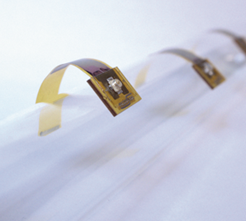
Nano Dimension Ltd., a leading Printed electronics (PE) / Additively Manufactured Electronics (AME) provider, announced today that its technology, DragonFly LDM system and materials were used to develop a 3D printed sealed packaging with electrical pads for Micro-Electromechanical Systems (MEMS).
The printed electronics package has the electrical pads directly printed on the metal layers on which an RF connector is soldered. The ability to transfer electric pads in a sealed package is one of the most crucial parts in ohmic-contact microelectromechanical systems (MEMS) as it determines the device performance and reliability, particularly for soft and flexible devices where the electrical connectors are typically difficult to produce.
“Nano Dimension’s AME technology helped us to achieve an original product prototype in which wires and connectors were eliminated such that the package was minimized to obtain an optimal user experience. It simplifies the manufacturing process compared to traditional manufacturing methods,” said Dr. Francesco Guido, CTO of Piezoskin S.R.L.
“With the DragonFly LDM 3D printer, Piezoskin can design customized printedpackages with flexible transducers, to meet their customers unique needs, drive innovation and get products to market faster,” said Mr. Yoav Stern, Nano Dimension’s CEO and President.
Share on:


Suggested Items
Warm Windows and Streamlined Skin Patches – IDTechEx Explores Flexible and Printed Electronics
04/26/2024 | IDTechExFlexible and printed electronics can be integrated into cars and homes to create modern aesthetics that are beneficial and easy to use. From luminous car controls to food labels that communicate the quality of food, the uses of this technology are endless and can upgrade many areas of everyday life.
iNEMI Packaging Tech Topic Series: Role of EDA in Advanced Semiconductor Packaging
04/26/2024 | iNEMIAdvanced semiconductor packaging with heterogenous integration has made on-package integration of multiple chips a crucial part of finding alternatives to transistor scaling. Historically, EDA tools for front-end and back-end design have evolved separately; however, design complexity and the increased number of die-to-die or die-to-substrate interconnections has led to the need for EDA tools that can support integration of overall design planning, implementation, and system analysis in a single cockpit.
Koh Young Showcases Award-winning Inspection Solutions at SMTconnect with SmartRep in Hall 4A.225
04/25/2024 | Koh Young TechnologyKoh Young Technology, the industry leader in True 3D measurement-based inspection solutions, will showcase an array of award-winning inspection and measurement solutions at SMTconnect alongside its sales partner, SmartRep, in booth 4A.225 at NürnbergMesse from June 11-13, 2023. The following offers a glimpse into what Koh Young will present at the tradeshow:
Real Time with… IPC APEX EXPO 2024: Plasmatreat: Innovative Surface Preparation Solutions
04/25/2024 | Real Time with...IPC APEX EXPOIn this interview, Editor Nolan Johnson speaks with Hardev Grewal, CEO and president of Plasmatreat, a developer of atmospheric plasma solutions. Plasmatreat uses clean compressed air and electricity to create plasma, offering environmentally friendly methods for surface preparation. Their technology measures plasma density for process optimization and can remove organic micro-contamination. Nolan and Hardev also discuss REDOX-Tool, a new technology for removing metal oxides.
Nanotechnology Market to Surpass $53.51 Billion by 2031
04/25/2024 | PRNewswireSkyQuest projects that the nanotechnology market will attain a value of USD 53.51 billion by 2031, with a CAGR of 36.4% over the forecast period (2024-2031).