


 The Chemical Connection: Onshoring PCB Production—Daunting but Certainly Possible
 It’s Only Common Sense: The Phone Is Still Mightier Than the Keyboard


ANSYS And Electro Magnetic Applications Partner To Deliver Design-To-Validation Workflow For Cable Harnesses
June 11, 2020 | PR NewswireEstimated reading time: 1 minute
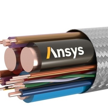
Electro Magnetic Applications, Inc. and Ansys are partnering to deliver an enhanced design-to-validation workflow for certifying cable harness models in aircraft and automobiles. The workflow greatly reduces electromagnetic interference (EMI) risks to cable harnesses, slashes development time, speeds certification and expedites new products to market faster than Cable harnesses that transmit electrical power and signals to electronics within aircraft and automobiles must be protected from external EMI sources such as high-intensity radiated fields (HIRF) and lightning strikes. To safeguard these vehicles against EMI interference, time-intensive and costly electromagnetic compatibility (EMC) certification testing must be conducted on physical prototypes.
EMA and Ansys' new workflow, Ansys EMA3D Cable, is a robust, platform-level EMC cable modeling solution for overcoming EMC design issues. When used early in the design stage, EMA3D Cable can increase the fidelity of an engineer's product performance predictions, reduce development costs and the need for physical prototyping and leverage test results as a basis for final acceptance and certification.
"EMA3D Cable enables engineers to efficiently assess complex cable harness system designs and evaluate protection schemes for vehicles of all sizes," said Dr. Timothy McDonald, president of EMA. "Partnering with Ansys on this dynamic new workflow will allow our mutual users to significantly enhance cable harness compatibility designs and substantially decrease cost and risk on the path to EMC certification."
"OEMs are designing new vehicles to be sleeker and lighter. This typically requires the removal of cable harness shielding, which creates EMI vulnerabilities," said Shane Emswiler, Ansys' senior vice president, physics business units. "Designing cable harnesses with EMA3D Cable will help engineers mitigate safety-critical EMI issues — including HIRF, lightning strikes, crosstalk and electromagnetic pulses—improving certification support and reducing design expenses."
Share on:


Testimonial
"We’re proud to call I-Connect007 a trusted partner. Their innovative approach and industry insight made our podcast collaboration a success by connecting us with the right audience and delivering real results."
Julia McCaffrey - NCAB GroupSuggested Items
Peters, Starteam, and Würth Elektronik Team Up For Digital Coating Technology
10/23/2025 | PetersUnder this heading, the PCB manufacturers Starteam and Würth Elektronik, along with Peters as inkjet coating supplier, have taken the initiative and worked together for months in trusting and target-oriented cooperation, to promote this innovative digital coating technology for solder resists and establish it on the market.
AI Triggers Next Paradigm Shift in PDN
10/23/2025 | Istvan Novak, SamtecArtificial intelligence (AI), together with machine learning (ML), is creating an unprecedented surge of computing and networking infrastructure needs. This, in turn, has dramatically increased the power consumption of computing and networking chips.
SEMICON Japan 2025 to Spotlight Sustainability in AI and Semiconductor Innovation
10/22/2025 | SEMISEMICON Japan 2025, the largest gathering of leaders from the microelectronics manufacturing supply chain in Japan, will bring together more than 1,200 exhibitors showcasing semiconductor solutions from December 17-19 at Tokyo Big Sight.
Zuken Announces ZIW Americas 2026 in Dallas
10/21/2025 | ZukenZuken USA, Inc., a global leader in electrical and electronic design automation, announced Zuken Innovation World (ZIW) Americas 2026, the company’s premier global conference dedicated to advancing the future of electrical and electronic product design. ZIW 2026 will be held June 9-11 in Dallas, Texas.
Keysight Completes Acquisition of Synopsys’ Optical Solutions Group and Ansys’ PowerArtist
10/17/2025 | Keysight Technologies, Inc.Keysight Technologies, Inc., announced the completion of its acquisitions of the Optical Solutions Group from Synopsys, Inc., and PowerArtist from Ansys, Inc.