


 Trouble in Your Tank: Understanding Interconnect Defects, Part 1
 It’s Only Common Sense: Marketing Isn’t Fluff, It’s Ammunition
 Driving Innovation: Mechanical and Optical Processes During Rigid-flex Production


Go Big: Limata’s X3000 Accurately Images Ultra-large, Flexible and Endless PCB Panels
October 22, 2020 | LimataEstimated reading time: 2 minutes
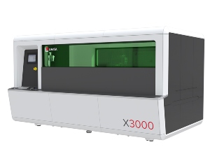
Limata, a provider of Laser Direct Imaging (LDI) systems for PCB manufacturing and adjacent markets, has launched the latest generation of its X3000 LDI system. This platform can handle the largest panels for dry-film patterning and solder mask imaging in PCB production without compromising on its highest precision standards in registration and resolution.
While standard PCB panel sizes have typically measured 24” x 18”, today there is an increasing demand for larger panels, often 24” x 36” or bigger, as well as a need to produce flexible PCBs in non-standard sizes. These large PCBs support a range of growing applications such as LED displays, 5G communications, aerospace and EV-automotive electronics. Using large PCBs instead of a combination of smaller boards delivers superior signal quality or lower signal attenuation in high frequency applications, while at the same time noticeably reducing assembly and installation costs.
Being able to handle large panel formats, up to 110" x 48", also means that the X3000 can simultaneously image multiple smaller PCBs in a single run, for example twelve standard 24" x 18" boards. This increases throughput, by reducing loading and unloading times, which further equates to reduced costs per panel. In addition, work processes can be set flexibly in manufacturing locations, since the X3000 can be loaded and unloaded from the front- and back-side.
"With the X3000, we have built an impressive system that can handle even the biggest oversize boards, whilst still retaining the outstanding accuracy of our X1000 and X2000 models," said Matthias Nagel, CTO of Limata. "In addition, the X3000 also supports roll-to-roll for the handling of endless flexible boards, with the largest PCB manufactured so far measuring 25 metres in length."
Auto-calibration
The X3000 model is market-proven and installed at multiple customer sites. This latest system generation further builds on the X-Series family's proven reliability, and utilizes an integrated auto-calibration system further delivering extremely high accuracy – unprecedented for a system of this size. The system improves registration quality with linear and nonlinear transformations, which are automatically applied in response to any distortion that it detects. In addition to PCB production, this accuracy makes the machine well-suited to applications such as chemical milling and industrial etching.
X3000 machine configurations are available with 2, 3 or 4 laser heads, providing a capacity of up to 24 ultra-violet (UV) lasers in total. A high resolution (HR) option provides an adjustable laser spot size for advanced HDI production, reliably handling dams and spaces down to 2 mil / 50 ?m. The platform uses cost-efficient high energy UV diode-lasers that achieve lifetimes (MTBF) of over 25,000 hours, thus further reducing TCO.
Faster solder mask imaging
Like all X-series system platforms from Limata, for solder mask direct imaging tasks the X3000 can also be equipped with Limata’s innovative LUVIR? technology, which uses a combination of UV and infrared (IR) lasers to reduce UV power consumption. Furthermore, this significantly increases the speed of solder mask (SM) direct imaging and achieves a TCO that is up to 40% lower than competing systems.
Share on:


Testimonial
"In a year when every marketing dollar mattered, I chose to keep I-Connect007 in our 2025 plan. Their commitment to high-quality, insightful content aligns with Koh Young’s values and helps readers navigate a changing industry. "
Brent Fischthal - Koh YoungSuggested Items
BTU International Earns 2025 Step-by-Step Excellence Award for Its Aqua Scrub™ Flux Management System
10/29/2025 | BTU International, Inc.BTU International, Inc., a leading supplier of advanced thermal processing equipment for the electronics manufacturing market, has been recognized with a 2025 Step-by-Step Excellence Award (SbSEA) for its Aqua Scrub™ Flux Management Technology, featured on the company’s Pyramax™ and Aurora™ reflow ovens.
On the Line With… Ultra HDI Podcast—Episode 7: “Solder Mask: Beyond the Traces,” Now Available
10/31/2025 | I-Connect007I-Connect007 is excited to announce the release of the seventh episode of its 12-part podcast series, On the Line With… American Standard Circuits: Ultra HDI. In this episode, “Solder Mask: Beyond the Traces,” host Nolan Johnson sits down with John Johnson, Director of Quality and Advanced Technology at American Standard Circuits, to explore the essential role that solder mask plays in the Ultra HDI (UHDI) manufacturing process.
Rehm Wins Mexico Technology Award for CondensoXLine with Formic Acid
10/17/2025 | Rehm Thermal SystemsModern electronics manufacturing requires technologies with high reliability. By using formic acid in convection, condensation, and contact soldering, Rehm Thermal Systems’ equipment ensures reliable, void-free solder joints — even when using flux-free solder pastes.
Indium Experts to Deliver Technical Presentations at SMTA International
10/14/2025 | Indium CorporationAs one of the leading materials providers to the power electronics assembly industry, Indium Corporation experts will share their technical insight on a wide range of innovative solder solutions at SMTA International (SMTAI), to be held October 19-23 in Rosemont, Illinois.
Knocking Down the Bone Pile: Revamp Your Components with BGA Reballing
10/14/2025 | Nash Bell -- Column: Knocking Down the Bone PileBall grid array (BGA) components evolved from pin grid array (PGA) devices, carrying over many of the same electrical benefits while introducing a more compact and efficient interconnect format. Instead of discrete leads, BGAs rely on solder balls on the underside of the package to connect to the PCB. In some advanced designs, solder balls are on both the PCB and the BGA package. In stacked configurations, such as package-on-package (PoP), these solder balls also interconnect multiple packages, enabling higher functionality in a smaller footprint.