


 The Chemical Connection: Reducing Etch System Water Usage, Part 2
 It’s Only Common Sense: Nice Guys Really Can Finish First
 The Right Approach: I Hear the Train A Comin'
LPKF Opens Cleanroom Fab
December 8, 2020 | LPKFEstimated reading time: 2 minutes
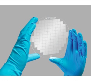
The technology company LPKF has now put a new cleanroom fab into operation to produce thin-glass components for applications in the electronics and semiconductor industry. The LIDE process (Laser Induced Deep Etching) developed by LPKF enables rapid and high-precision structuring of thin glass without impairing surface properties. The original stability of the glass remains fully intact. This process facilitates the use of glass in, for example, the production of microsystems, sensors, display components, and microchips.
The cleanroom fab was constructed in record time. Due to the considerable interest shown by the semiconductor and electronics industry in this innovative method of processing thin glass, rapid completion was required. Despite the difficult circumstances encountered this year with travel restrictions among service providers and delivery issues involving some manufacturers, the fab was constructed within a tight schedule of just 13 months. Dirk Neizel, Operations Manager at LPKF, was the driving force behind organizing and expediting the construction. “We now have a very flexible hall that we can equip in accordance with customer requirements, thus allowing the required production processes in each case to be offered as quickly as possible. With a complete air exchange every 60 seconds and precisely controllable climatic conditions, the fab optimally meets all the requirements of a production cleanroom. We have also invested heavily in modern safety technology in all systems and laboratories,” emphasizes Dirk Neizel.
Dr. Roman Ostholt heads the Electronics Business Unit, which also includes the LIDE service division under the brand name Vitrion. “We can now produce large quantities of thin-glass components and micro-components quickly and efficiently in our foundry and supply our customers worldwide,” he reports. Together with his team, he will continue to intensify and develop the cooperation with customers and partners in the semiconductor and electronics industry. In addition to the sale of its systems, this foundry constitutes a significant extension to LPKF's business model.
For CEO Dr. Götz M. Bendele, the project is indicative of LPKF's innovative strength and customer proximity: “Our new fab enables easy access to our technology for a broad set of customers across industries, who from today can order structured thin glass components from LPKF for their high-volume applications. In doing so, they can quickly realize substantial value from our transformative platform technology, without the need to invest in both systems and process capabilities. This drives our customers’ competitive advantage.”
Glass is a material of particular interest to many areas in the electronics and semiconductor sector due to its properties. For a long time, the material was considered very difficult to work with. Surface defects associated with the production process have earned glass the reputation of being prone to brittle fracture and therefore, at best, suitable for simple tasks only. Thanks to Laser Induced Deep Etching technology (LIDE), deep microstructures can now be created in glass for the first time without causing micro cracks, stresses, or other surface defects.
Processing is extremely precise, and the process is fast. Interest in using this inexpensive material is increasing at a corresponding rate. With the use of LIDE-processed glass, even better results than previously possible can now be achieved, for example, in advanced IC and wafer level packaging in heterogeneous integration. The process also opens up new opportunities for processing and using display glass or microfluidic arrays.
Share on:


Suggested Items
I-Connect007 Editor’s Choice: Five Must-Reads for the Week
05/03/2024 | Nolan Johnson, I-Connect007This week’s most important news is strategic—and telling. When one puts together the IPC industry reports, we simply have to include the recent conversation with Shawn DuBravac and Tom Kastner. On the design side, check out the latest “On The Line With…” podcast featuring Brad Griffin from Cadence Design Systems, discussing SI and PI in the realm of intelligent system design.
IMI Welcomes New CEO
05/03/2024 | IMIIntegrated Micro-Electronics, Inc. (IMI),The IMI Board of Directors announced, in a disclosure dated April 25, 2024, the appointment of Louis Sylvester Hughes, Chief Executive Officer (CEO).
Electronics Industry Sentiment Rose in April, Hitting New High
05/02/2024 | IPCApril 2024 marked the third consecutive month of sentiment growth among electronics manufacturers. When asked if they expected labor costs for hourly workers to rise over the next month, manufacturers in the United States, Mexico, and Europe predicted a five percent increase, while manufacturers in Asia predicted a slightly lower four percent increase.
iNEMI Names Grace O'Malley CTO
05/02/2024 | iNEMIThe Board of Directors of the International Electronics Manufacturing Initiative (iNEMI) has named Grace O'Malley Chief Technical Officer (CTO).
ZESTRON Academy Launches 2024 Advanced Packaging & Power Electronics Webinar Series
05/01/2024 | ZESTRONZESTRON, the leading global provider of high-precision cleaning products, services, and training solutions in the electronics manufacturing and semiconductor industries, proudly announces the launch of its highly anticipated webinar series on Advanced Packaging & Power Electronics, a webinar series on the latest innovations, cleaning, and corrosion challenges.