


 Dan’s Biz Bookshelf: ‘Abundance: How We Build a Better Future’
 Trouble in Your Tank: In Complex Systems, Design Rules Aren’t Optional
 It’s Only Common Sense: The Phone Is Still Your Competitive Advantage


Averatek to Present 'Surface Treatment for Soldering Aluminum PCBs to Conventional Copper PCBs' at IPC APEX EXPO
October 29, 2021 | AveratekEstimated reading time: 2 minutes
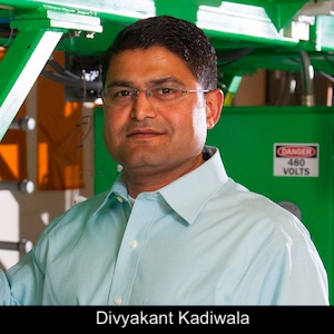
Averatek is pleased to announce that VP of Manufacturing Divyakant Kadiwala will present the paper entitled, “Surface Treatment for Soldering Aluminum PCBs to Conventional Copper PCBs” during the IPC APEX EXPO Technical Conference, scheduled to take place Jan. 22-27, 2022 at the San Diego Convention Center in California. The paper was co-authored by Nazarali Merchant, Ph.D., Senior Materials Scientist for Averatek.
Soldering is the preferred method for mounting SMDs and connecting circuit boards. But that brings in processing challenges. Soldering to aluminum requires an additional surface treatment or the use of conductive epoxy. These are cost-prohibitive and have reliability challenges and existing products like solders, fluxes, tack agents, cleaners etc. are formulated for Cu-PCBs and do not work on aluminum.
An advanced surface treatment technology will be presented that addresses all these constraints. Once printed on aluminum using conventional printing techniques such as screen, stencil etc., it is cured thermally in a convection oven at low temperatures, leaving a non-conductive deposit on the pads. This is followed by conventional process i.e. print solder over the treated pads, place components and then reflow resulting in finished Al-PCBs. It can also be used to solder Al-PCBs to flexible and rigid Cu-PCBs.
This is a paradigm shift in the industry which opens up many new applications, including those in the RFID, LED, and automotive industries. We will show solder cross-sections and shear data on the soldered joints, including Al-PET to Cu-PCB, Al-PET to Cu-Polyimide using aluminum metallization with low temperature Bi-Sn-Ag solders.
Kadiwala is a process development and project management leader in developing innovative products from laboratory concepts to large-scale manufacturing. He has 15+ years of multi-national experience with utilizing emerging technologies in strategic roles.
Kadiwala holds a BS in Chemical Engineering from the University of Mumbai, and a Master’s degree in Manufacturing Systems Engineering from the University of Wisconsin.
Merchant has 20 years of successful deliverables in PCBs, semiconductor packaging, metallurgy, welding consumables and processes, superconductors, fuel cells, batteries, solar cells, and failure analysis. His work has resulted in six US patents, three US patent applications under review, and 25 technical publications.
Merchant holds Doctorate and Master’s degree in Materials Engineering from the University of Illinois, and a Bachelor of Technology in Metallurgical Engineering from IIT of Bombay.
Share on:


Testimonial
"The I-Connect007 team is outstanding—kind, responsive, and a true marketing partner. Their design team created fresh, eye-catching ads, and their editorial support polished our content to let our brand shine. Thank you all! "
Sweeney Ng - CEE PCBSuggested Items
SPEA Expands Global Footprint with New Hub in Santa Clara, Silicon Valley
05/08/2026 | SPEASPEA has officially landed in the heart of Silicon Valley, with the grand opening of its newest facility in Santa Clara, California.
Nano Dimension Reports 106% YoY Revenue Growth in Q1 2026
05/08/2026 | Nano DimensionNano Dimension Ltd., a leader in digital manufacturing solutions, announced financial results for the first quarter ended March 31, 2026.
AI Demand Drives PCB Material Market Growth
05/08/2026 | TPCAAs AI computing continues to drive a comprehensive upgrade in hardware specifications, the global printed circuit board industry is undergoing a profound structural transformation.
Zhen Ding April 2026 Revenue Hits Record High on Strong AI Demand
05/07/2026 | Zhen Ding TechnologyZhen Ding Technology Holding Limited, a global leading PCB manufacturer, reported April 2026 revenue of NT$15,196 million, up 11.83% YoY, reaching a record high for the same period in the company’s history.
ICAPE Group Reports Q1 2026 Revenue of €51.5 Million
05/06/2026 | ICAPE GroupQ1 2026 revenue of €51.5 million, up 2.2% compared to Q1 2025 (up +20% compared to Q1 2024), and up 4.6% compared to Q4 2025