


 SMT Perspectives and Prospects: Warren Buffett’s Perpetual Wisdom, Part 1
 Standard of Excellence: Training Your Team to Excel in Customer Service
 Smart Automation: What Industry 4.0 Means for Mid-sized Electronics Manufacturing


Saki Corporation Launches Next-generation 3D AOI System
May 24, 2022 | Saki CorporationEstimated reading time: 1 minute
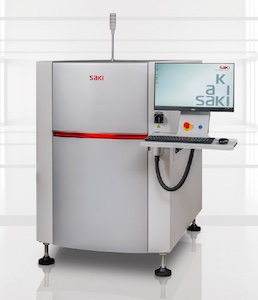
Saki Corporation, an innovator in the field of automated optical and X-ray inspection equipment, has developed the new 3Di series of high-speed, high-precision, next-generation in-line 3D automated optical inspection (3D AOI) systems for complex inspection of high-density printed circuit boards and boards with a combination of very small and tall components. The new 3Di series is equipped with a newly developed camera system that significantly reduces cycle and produces ultra-sharp high-resolution 3D images thanks to its ability to simultaneously and accurately inspect both extremely small parts, such as 008004s (0201 metric), and tall parts at the same time. This latest automated inspection solution from Saki contributes to enhanced quality assurance and increased productivity and is perfect for highest quality inspection of ever-evolving high-density PCB technology.
Saki will debut the first AOI machine in this new 3Di series at the 23rd JISSO PROTEC 2022 show (June 15-17, Tokyo Big Sight International Exhibition Center, Japan). The machine configuration will feature a camera resolution of 8 ?m, a height measurement range of 25 mm, and an imaging speed of 4,500 mm2/s. The Saki team is looking forward to welcoming show visitors to booth 4D-12 in East Hall 4-6.
Key features of the new 3Di series include:
1. A newly developed high-resolution camera system that enables:
- high-resolution inspection of high-density PCBs and ultra-small components.
- expanded height measurement range.
2. Sophisticated software and hardware configuration that optimizes image processing and achieves the industry’s fastest cycle time.
3. An innovative and unique inspection algorithm that enables clear 3D solder joint inspection.
4. Scalability with the option to easily modify configurations at any time as required by adding new camera heads, AI functions, and other future features.
Norihiro Koike, President and CEO of Saki Corporation, commented: “Saki's new 3Di series keeps pace with the rapidly evolving needs of the market and delivers highest inspection quality and accuracy along with the fast cycle times demanded by the next generation of PCB technology. We will continue to develop add-on solutions in the future that will provide a variety of additional optional functions, offer flexibility, and contribute to sustainable manufacturing concepts that that are shaping our customers' smart factories. In addition to our own booth at JISSO PROTEC 2022, our latest AOI solution will also be showcased by Panasonic Connect Corporation on Booth No. 5D-29. We look forward to seeing you at the exhibition."
Share on:


Testimonial
"The I-Connect007 team is outstanding—kind, responsive, and a true marketing partner. Their design team created fresh, eye-catching ads, and their editorial support polished our content to let our brand shine. Thank you all! "
Sweeney Ng - CEE PCBSuggested Items
MacDermid Alpha Electronics Solutions Unveils Unified Global Website to Deepen Customer, Talent, and Stakeholder Engagement
07/31/2025 | MacDermid Alpha Electronics SolutionsMacDermid Alpha Electronics Solutions, the electronics business of Elements Solutions Inc, today launched macdermidalpha.com - a unified global website built to deepen digital engagement. The launch marks a significant milestone in the business’ ongoing commitment to delivering more meaningful, interactive, and impactful experiences for its customers, talent, and stakeholders worldwide.
KOKI to Showcase Analytical Services and New HF1200 Solder Paste at SMTA Guadalajara 2025
07/31/2025 | KOKIKOKI, a global leader in advanced soldering materials and process optimization services, will exhibit at the SMTA Guadalajara Expo & Tech Forum, taking place September 17 & 18, 2025 at Expo Guadalajara, Salón Jalisco Halls D & E in Guadalajara, Mexico.
Weller Tools Supports Future Talent with Exclusive Donation to SMTA Michigan Student Soldering Competition
07/23/2025 | Weller ToolsWeller Tools, the industry leader in hand soldering solutions, is proud to announce its support of the upcoming SMTA Michigan Expo & Tech Forum by donating a limited-edition 80th Anniversary Black Soldering Set to the event’s student soldering competition.
Koh Young Appoints Tom Hattori as President of Koh Young Japan
07/21/2025 | Koh YoungKoh Young Technology, the global leader in True 3D measurement-based inspection solutions, announced the appointment of Tom Hattori as President of Koh Young Japan (JKY).
Silicon Mountain Contract Services Enhances SMT Capabilities with New HELLER Reflow Oven
07/17/2025 | Silicon Mountain Contract ServicesSilicon Mountain Contract Services, a leading provider of custom electronics manufacturing solutions, is proud to announce a significant upgrade to its SMT production capability with the addition of a HELLER 2043 MK5 10‑zone reflow oven to its Nampa facility.