


 The Marketing Minute: Marketing With Layers
 The Right Approach: Electro-Tek—A Williams Family Legacy, Part 1
 It’s Only Common Sense: If You’re Not Differentiated, You’re Dead


Bowman's Micro XRF Measures Smallest Features in Wafers, Microelectronics
June 6, 2022 | BowmanEstimated reading time: 1 minute
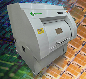
Bowman has introduced an important addition to its suite of precision XRF instruments used in the PCB, semiconductor and microelectronics industries.
The Bowman A Series Micro XRF quickly measures the smallest features on semiconductors and microelectronics. It accommodates very large PCB panels, and wafers of any size, for full sample coverage and multi-point programmable automation.
Poly-capillary optics focus the X-ray beam to 7.5 µm FWHM, the world’s smallest for XRF coating thickness analysis. A 140X magnification camera measures features on that scale; a secondary, low magnification camera provides live-viewing of samples and “birds-eye” macro-view imaging. Bowman’s proprietary dual-camera system lets operators see the entire part, click the image to zoom with the high-mag camera, and quickly identify the feature of interest.
A programmable X-Y stage with movement of 23.6 in (600 mm) in each direction can handle the largest samples in the industry. The stage has precision down to +/- 1 µm for each axis, and is used to select and measure multiple points; Bowman pattern recognition software and auto-focus features also do this automatically. The system’s 3D mapping capability can be used to view the topography of ENIG, ENEPIG, EPIG and other elite processes.
A Series instruments include 7.5 µm optics with molybdenum anode tube (chromium and tungsten also available) and a high-resolution, large-window Silicon Drift Detector (SDD) which processes more than 2 million counts per second. SDDs are the standard, industry-wide, for complex thin films. The high count rate capability is key to achieving a low minimum detection limit (MDL) and highest spectral resolution.
A Series systems are distinctive in that they are cleanroom-ready, have the largest semiconductor stage movement on the market, and are supported worldwide by a service network that provides same-day response for every benchtop XRF requirement. Equipment evaluation, selection, commissioning, maintenance and modernization is available for users of Bowman instruments, as well as other major XRF brands.
Share on:


Testimonial
"Our marketing partnership with I-Connect007 is already delivering. Just a day after our press release went live, we received a direct inquiry about our updated products!"
Rachael Temple - AlltematedSuggested Items
Smart Eye Collaborates with Sony on Next-Generation Interior Sensing and Iris Authentication
10/09/2025 | Smart EyeSmart Eye AB, the global leader in Interior Sensing AI and Driver Monitoring Systems (DMS), announced a collaboration with Sony Semiconductor Solutions Corporation (Sony) to integrate Smart Eye’s interior sensing and biometric authentication software with Sony’s newly released IMX775 RGB-IR image sensor.
SEMICON Europa 2025 to Highlight Innovations in Advanced Packaging, Fab Management, and MEMS and Imaging Sensors to Bolster Europe’s Semiconductor Resilience
10/03/2025 | SEMISemiconductor industry experts will convene at SEMICON Europa 2025, November 18-21 at Messe München in Munich, to explore the latest trends and innovations in advanced packaging and fab management.
MEMS & Imaging Sensors Summit to Spotlight Sensing Revolution for Europe’s Leadership
09/11/2025 | SEMIIndustry experts will gather November 19-20 at the SEMI MEMS & Imaging Sensors Summit 2025 to explore the latest breakthroughs in AI-driven MEMS and imaging optimization, AR/VR technologies, and advanced sensor solutions for critical defence applications.
Direct Imaging System Market Size to Hit $4.30B by 2032, Driven by Increasing Demand for High-Precision PCB Manufacturing
09/11/2025 | Globe NewswireAccording to the SNS Insider, “The Direct Imaging System Market size was valued at $2.21 Billion in 2024 and is projected to reach $4.30 Billion by 2032, growing at a CAGR of 8.68% during 2025-2032.”
I-Connect007’s Editor’s Choice: Five Must-Reads for the Week
07/04/2025 | Marcy LaRont, I-Connect007For our industry, we have seen several bullish market announcements over the past few weeks, including one this week by IDC on the massive growth in the global server market. We’re also closely watching global trade and nearshoring. One good example of successful nearshoring is Rehm Thermal Systems, which celebrates its 10th anniversary in Mexico and the official opening of its new building in Guadalajara.