


 The Marketing Minute: Marketing With Layers
 The Right Approach: Electro-Tek—A Williams Family Legacy, Part 1
 It’s Only Common Sense: If You’re Not Differentiated, You’re Dead


Ucamco Adds In-house Production of Large and Extra Large 'Bird of Prey' Photoplotters
June 17, 2022 | UcamcoEstimated reading time: 1 minute
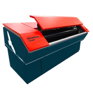
Ucamco has added the in-house production, from scratch, of new large and extra-large format laser photoplotters to its capabilities.
As the market leader in not only photoplotters, but also PCB CAM and Pre-CAM Software and Direct Imaging Systems, Ucamco is committed to keep developing PCB technology. Even more, Ucamco invests in it: "Ucamco is an expert in the field. We love to take on challenges", says Michel Van den heuvel, Product Imaging Group Director at Ucamco. "We figured we have all the human and material resources in-house to successfully build large and extra-large photoplotters. Add that to the ever-growing importance of providing full-service solutions for our customers, and the addition of this production line has really been a no-brainer.
"Our (extra) large format photoplotters are external drum laser plotters with an automatic film loader and online connection to the film processor. One of the main qualities of an excellent photoplotter is having a state-of-the-art optical-mechanical imaging unit."
"You could argue that our plotters possess the same sharp eyesight as birds of prey. Which is why we have named our brand new machines after birds with the larges wingspan - Hawk and Condor - obviously due to the size of the photoplotters."
Share on:


Testimonial
"The I-Connect007 team is outstanding—kind, responsive, and a true marketing partner. Their design team created fresh, eye-catching ads, and their editorial support polished our content to let our brand shine. Thank you all! "
Sweeney Ng - CEE PCBSuggested Items
Smart Eye Collaborates with Sony on Next-Generation Interior Sensing and Iris Authentication
10/09/2025 | Smart EyeSmart Eye AB, the global leader in Interior Sensing AI and Driver Monitoring Systems (DMS), announced a collaboration with Sony Semiconductor Solutions Corporation (Sony) to integrate Smart Eye’s interior sensing and biometric authentication software with Sony’s newly released IMX775 RGB-IR image sensor.
SEMICON Europa 2025 to Highlight Innovations in Advanced Packaging, Fab Management, and MEMS and Imaging Sensors to Bolster Europe’s Semiconductor Resilience
10/03/2025 | SEMISemiconductor industry experts will convene at SEMICON Europa 2025, November 18-21 at Messe München in Munich, to explore the latest trends and innovations in advanced packaging and fab management.
MEMS & Imaging Sensors Summit to Spotlight Sensing Revolution for Europe’s Leadership
09/11/2025 | SEMIIndustry experts will gather November 19-20 at the SEMI MEMS & Imaging Sensors Summit 2025 to explore the latest breakthroughs in AI-driven MEMS and imaging optimization, AR/VR technologies, and advanced sensor solutions for critical defence applications.
Direct Imaging System Market Size to Hit $4.30B by 2032, Driven by Increasing Demand for High-Precision PCB Manufacturing
09/11/2025 | Globe NewswireAccording to the SNS Insider, “The Direct Imaging System Market size was valued at $2.21 Billion in 2024 and is projected to reach $4.30 Billion by 2032, growing at a CAGR of 8.68% during 2025-2032.”
I-Connect007’s Editor’s Choice: Five Must-Reads for the Week
07/04/2025 | Marcy LaRont, I-Connect007For our industry, we have seen several bullish market announcements over the past few weeks, including one this week by IDC on the massive growth in the global server market. We’re also closely watching global trade and nearshoring. One good example of successful nearshoring is Rehm Thermal Systems, which celebrates its 10th anniversary in Mexico and the official opening of its new building in Guadalajara.