


 Learning With Leo: UHDI—The Next Leap in PCB Manufacturing
 Nolan’s Notes: Is Mexico the Pulse of Electronics in the Americas?
 Standard of Excellence: Speed vs. Quality in Customer Service


Altus Assists PCB Specialists to Add Best-in-Class Inspection to its Production Line
April 11, 2023 | Altus GroupEstimated reading time: 2 minutes
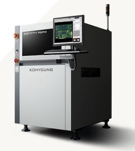
To ensure quality and efficiency are implemented at all times and compete as a best-in-class CEM, Garner Osborne Circuits liaised with capital equipment supplier and service provider Altus to further enhance their inspection processes through 3D AOI technology.
False calls and escapes are unavoidable when using 2D inspection techniques. When manufacturing complex miniaturised PCBs, this assessment method cannot meet the high standards critical to the success and performance of modern electronic devices. Identifying defects early in assembly and having data to support process improvement decisions is vital to ensure quality. Therefore, moving away from 2D inspection methods to 3D AOI technology is crucial.
To take their inspections processes to a new level Altus introduced Garner Osborne to Koh Young Zenith Alpha HS+, the foremost true 3D AOI solution powered by AI enhanced high speed 3D measurement capabilities. The system incorporates KSMART technology which revolutionises data collection and analysis, and improves PCB process optimisation.
Steve Honeybun, CEM Operations Director, Garner Osborne, said: ‘’Garner Osborne has always had a philosophy of continuous improvement to consistently perform at the top end of electronic production services. Moving to a 3D light metrology process with Koh Young, who is widely regarded as the best inspection provider in the market, is a great reflection of that.
“We have worked with Altus for several years, and extending our partnership further, given the support they have always given us, made the decision easier. As a result, we now have fully 3D SPI and AOI to support improving our production yields, and we are delighted to get the unit up and running.’’
KSMART analysis collects all inspection and measurement data and helps advanced inspection systems evolve from “Pass/Fail” tools into highly intuitive, dynamic decision-making systems. Adept equipment supplies can then apply the data set to proprietary AI engines for continuous performance improvement. KSMART ensures the highest levels of transparency by showing all conditions of the lines, while providing the required documentation for changes to each job for traceability.
Anthony Oh, Altus Technical Applications Manager: ‘’This has been an excellent project for Altus, and we especially enjoy working with the team at Garner Osborne. Of course, we take each project as a standalone in its own right, and their team tested us, given that by upgrading to Koh Young, they moved away from an already trusted partner. I am pleased that we demonstrated our claims of providing the lowest levels of false calls available and showing the value of fully 3D light measurement data collection to improve yield. This aspect is where CEM customers can unlock value in their production environment and for their customers.’’
Share on:


Testimonial
"Your magazines are a great platform for people to exchange knowledge. Thank you for the work that you do."
Simon Khesin - Schmoll MaschinenSuggested Items
Trouble in Your Tank: Understanding Interconnect Defects, Part 1
11/04/2025 | Michael Carano -- Column: Trouble in Your TankThis month, I’ll address interconnect defects (ICDs). While this defect continues to rear its ugly head, don’t despair. There are solutions, most of which center on process control and understanding the relationship of the chemistry, materials, and equipment. First, though, let’s discuss ICDs.
Unlocking the Promise of AI in Electronics Manufacturing
10/29/2025 | Shobhit Agrawal, Keysight TechnologiesThe electronics manufacturing industry is rapidly evolving as more complicated products are introduced in the production lines, which require technological advancements even in the production processes. The requirements for production that is efficient, product quality that is greater, and product life cycles that are shorter are more crucial than ever before. In the electronic device life cycle, from design to maintenance, test phases have a significant impact on the economy of the company. Test processes are closely linked to the production volume and impacted by the complexity of the product. For businesses to maintain their competitive edge, they need to adopt innovative solutions and redefine processes.
Connect the Dots: Designing for the Reality of UHDI PCBs—Drilling
11/04/2025 | Matt Stevenson -- Column: Connect the DotsUltra high density interconnect (UHDI) PCBs are changing the game in designing for the reality of manufacturing. With both consumer and industrial electronic devices becoming more advanced, the demand for UHDI PCBs will grow. That means we’re all likely to be designing more UHDI boards. UHDI advanced miniaturization technology challenges designers with regard to both board thickness and footprint. Designers will face more variables in every aspect of design creation. This is certainly the case with drilling.
Driving Innovation: Mechanical and Optical Processes During Rigid-flex Production
10/28/2025 | Kurt Palmer -- Column: Driving InnovationRigid-flex printed circuit boards are a highly effective solution for placing complex circuitry in tight, three-dimensional spaces. They are now indispensable across a range of industries, from medical devices and aerospace to advanced consumer electronics, helping designers make the most efficient use of available space. However, their unique construction—combining rigid and flexible materials—presents a fundamental challenge for PCB manufacturers.
SMTAI 2025 Review: Reflecting on a Pragmatic and Forward-looking Industry
10/27/2025 | Marcy LaRont, I-Connect007Leaving the show floor on the final afternoon of SMTA International last week in Rosemont, Illinois, it was clear that the show remains a grounded, technically driven event that delivers a solid program, good networking, and an easy space to commune with industry colleagues and meet with customers.