-

- News
- Books
Featured Books
- smt007 Magazine
Latest Issues
Current Issue
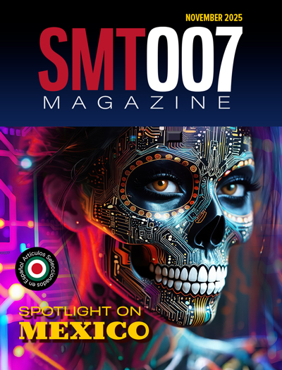
Spotlight on Mexico
Mexico isn’t just part of the electronics manufacturing conversation—it’s leading it. From growing investments to cross-border collaborations, Mexico is fast becoming the center of electronics in North America. This issue includes bilingual content, with all feature articles available in both English and Spanish.

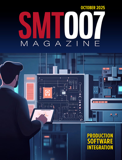
Production Software Integration
EMS companies need advanced software systems to thrive and compete. But these systems require significant effort to integrate and deploy. What is the reality, and how can we make it easier for everyone?

Spotlight on India
We invite you on a virtual tour of India’s thriving ecosystem, guided by the Global Electronics Association’s India office staff, who share their insights into the region’s growth and opportunities.
- Articles
Article Highlights
- Columns
- Links
- Media kit
||| MENU - smt007 Magazine
Advice to the Learner
May 3, 2023 | Barry Matties, I-Connect007Estimated reading time: 5 minutes
Barry Matties chats with Dale Lee and Alexander Noggle, a college student attending the SMTA Houston Expo & Tech Forum, about the need to listen to the past but keep an eye on the future, especially when it comes to understanding technology. For now, Dale says, get out and gain as much industry experience as possible.
Barry Matties: I’m here with student Alexander Noggle, and Dale Lee, who has 40 years of industry experience. Alexander, would you briefly describe yourself and what you are currently doing?
Alexander Noggle: I’m an electrical engineering student at the University of North Texas, and I’m really interested in power systems. I’ve noticed that among analog circuit designers, there are many older people. This presents a great job opportunity and outlook for younger people.
Matties: I agree with you about the job opportunities. Is that why you’re here attending the SMTA Houston Expo?
Noggle: This is my first conference. As a student, I’m trying to get more involved in the industry, learn as much as I can, and find job opportunities.
Matties: You’re in electrical engineering. Do you hope to become a circuit designer?
Noggle: Yes, I think so. I have an internship lined up at Texas Instruments, where I will be working with power systems.
Matties: Dale, what advice would you give a young student?
Dale Lee: The more industry experience you can get, the better off you’ll be. Definitely take time to talk off-topic with some of the senior people in the industry; they’ve been around before we had automated tools. Learn what they saw and experienced before having the design tools we now have available. While most of us have no idea where the information in the CAD tool came from, these older people do. They can tell you exactly where that information came from—and even where there are holes or gaps in that information. This is critical. Once you understand the gaps, you can understand how to use them to your advantage and how they can hinder your designs.
Matties: The title of Dale’s presentation today was “DFM [Design for Manufacturing] … Is it Dead or Alive?” What does DFM mean to you, and do you think it’s dead or alive?
Lee: The term started in the late 1970s and early 1980s, when automation came into the electronics assembly world. Automated assembly equipment, mainly component insertion tools, had requirements such as certain hole sizes. Then wave solder became a big deal, and we suddenly had soldering rules for wave solder.
Technologies grew. By the ’80s, IBM introduced this little thing called the personal computer. CAD tools started to shrink because we wanted to get more data into the tools. Then surface mount came out, which was a new evolution. It evolved rapidly, unlike through-hole, which took decades to learn and develop, mostly because everything, even board design, was done on paper. (I can even remember the days when we taped them out and peeled them off.)
Now, packaging technologies, the functional requirements of the design, exceed anything we can do simply by doing a surface analysis. But you’ve got to understand everything in three dimensions and in motion, which is the hardest part.
Matties: Now we turn it around and call it manufacturing for design, rather than design for manufacturing. Is it a new trend?
Lee: Yes, it is new. It’s formalizing it, but we’ve been doing it in bits and pieces for many years. Now we don’t do a standard stencil. Every time we look at a stencil, we have to figure out whether to oversize or undersize, do step-ups or step-downs. You are customizing your manufacturing process to the assembly. Some people are doing offsets of parts to reduce voiding because they understand how they move.
A lot of things like that are happening. With RF designs, trace routings are extremely critical. You need to understand how you can restrict part movements. Rather than using traditional solder mask, which can cause RF problems, there are technologies available to help design your manufacturing process to meet functional requirements of products. You can also change how the board is fabricated.
We are getting to the point where design densities are so great that no rework or touch-up is allowed. It’s either good or scrap. So, you really need to understand everything about design to ensure that your manufacturing process meets all the requirements, because there is no rework, no touch-up allowed.
Matties: Alexander, one thing that we hear often is that designers need to understand the PCB manufacturing process in a deeper way. There are several great fabricating shops around here. Have you considered getting a job with a PCB fabricator to really learn the process?
Noggle: It would give me a huge advantage. However, I think I would prefer to just take a university course on it, rather than spend a year at a company learning about PCB design. I think it would save me time.
Matties: Dale, without exaggeration, the one thing we hear all the time is, “We wish designers understood the bare board manufacturing process more.” Those that do understand it have a huge financial and technological advantage.
Lee: The bare board industry is getting so complex because their designs are getting so complex. We are actually embedding functional elements, active and passive, into boards. Also, traces on boards are getting down to less than 10 microns—less than a half-thousandth of an inch. That’s the semiconductor world from 40 years ago.
Today, dust elements in manufacturing are becoming greater and greater defects. Yet, what’s the number one paper/FOD issue in the manufacturing floor? Passive devices, because they’re still coming on punch paper tape.
Lee: Alexander, if you ever get a chance to visit both a prototype board shop and a volume production board shop, I recommend you do. You’ll see a night-and-day difference, but all the processes are the same.
Matties: Whether you’re building one or a million.
Lee: Right. Once you realize it’s the same thing with just larger tanks and conveyors.
Matties: Great. Thank you so much for your time. Thank you.
Noggle: Thank you.
Lee: You’re very welcome.
Testimonial
"The I-Connect007 team is outstanding—kind, responsive, and a true marketing partner. Their design team created fresh, eye-catching ads, and their editorial support polished our content to let our brand shine. Thank you all! "
Sweeney Ng - CEE PCBSuggested Items
BTU International Earns 2025 Step-by-Step Excellence Award for Its Aqua Scrub™ Flux Management System
10/29/2025 | BTU International, Inc.BTU International, Inc., a leading supplier of advanced thermal processing equipment for the electronics manufacturing market, has been recognized with a 2025 Step-by-Step Excellence Award (SbSEA) for its Aqua Scrub™ Flux Management Technology, featured on the company’s Pyramax™ and Aurora™ reflow ovens.
On the Line With… Ultra HDI Podcast—Episode 7: “Solder Mask: Beyond the Traces,” Now Available
10/31/2025 | I-Connect007I-Connect007 is excited to announce the release of the seventh episode of its 12-part podcast series, On the Line With… American Standard Circuits: Ultra HDI. In this episode, “Solder Mask: Beyond the Traces,” host Nolan Johnson sits down with John Johnson, Director of Quality and Advanced Technology at American Standard Circuits, to explore the essential role that solder mask plays in the Ultra HDI (UHDI) manufacturing process.
Rehm Wins Mexico Technology Award for CondensoXLine with Formic Acid
10/17/2025 | Rehm Thermal SystemsModern electronics manufacturing requires technologies with high reliability. By using formic acid in convection, condensation, and contact soldering, Rehm Thermal Systems’ equipment ensures reliable, void-free solder joints — even when using flux-free solder pastes.
Indium Experts to Deliver Technical Presentations at SMTA International
10/14/2025 | Indium CorporationAs one of the leading materials providers to the power electronics assembly industry, Indium Corporation experts will share their technical insight on a wide range of innovative solder solutions at SMTA International (SMTAI), to be held October 19-23 in Rosemont, Illinois.
Knocking Down the Bone Pile: Revamp Your Components with BGA Reballing
10/14/2025 | Nash Bell -- Column: Knocking Down the Bone PileBall grid array (BGA) components evolved from pin grid array (PGA) devices, carrying over many of the same electrical benefits while introducing a more compact and efficient interconnect format. Instead of discrete leads, BGAs rely on solder balls on the underside of the package to connect to the PCB. In some advanced designs, solder balls are on both the PCB and the BGA package. In stacked configurations, such as package-on-package (PoP), these solder balls also interconnect multiple packages, enabling higher functionality in a smaller footprint.


