


 It’s Only Common Sense: If You’re Not Differentiated, You’re Dead
 Alpha Insights, Performance by Design: The Future of PCB Manufacturing in the Midwest
 Happy’s Tech Talk #43: Engineering Statistics Training With Free Software


Ucamco's LeVina: Direct Imaging for Next-gen Packaging Substrates
November 14, 2023 | UcamcoEstimated reading time: 1 minute
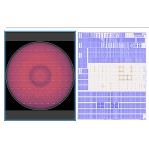
Ucamco is proud to introduce LeVina to the European market. LeVina is the perfect Direct Imaging solution for next-gen packaging substrates.
Just like Ledia direct imagers, LeVina is Japanese technology made by SCREEN.
World-leading imaging of 2 µm
LeVina combines superior imaging heads equipped with SCREEN’s proprietary GLVTM optical engine and laser control technologies that utilize an optical system featuring more of SCREEN’s unique expertise. This new system is specifically designed for mass production and enables direct imaging of substrates at a market-leading resolution of 2/2 μm L/S. It will continue to deliver high-definition patterning of advanced packages even as they become increasingly miniaturized.
Throughput of 100 substrates per hour with L/S = 5/5 µm
LeVina is fitted with an extremely reliable multi-head system and stage capable of moving at up to 480 millimeters per second. Alignment marks are read during scanning, allowing outstanding throughput regardless of the number of marks in the scanning direction (can also be automated). These features enable high resolution processing up to 100 substrates (510 x 515 mm) per hour at L/S = 5/5 μm.
Low running costs
Thanks to the laser diodes used in its light source, LeVina cuts operating costs by around 70%.
Improved cleanness
With LeVina, sources of particle generation have been blocked and it has been equipped with airflow control technologies that have a proven record in cleaning equipment for the semiconductor market. These advances have reduced contamination inside the system, helping to significantly improve yields.
Learn more at Productronica
Ucamco will feature a testing panel of LeVina at Productronica in Munich next week, November 14-17. Visit us in hall B3, booth 425 to learn more about this ground-breaking technology.
Share on:


Testimonial
"The I-Connect007 team is outstanding—kind, responsive, and a true marketing partner. Their design team created fresh, eye-catching ads, and their editorial support polished our content to let our brand shine. Thank you all! "
Sweeney Ng - CEE PCBSuggested Items
Imec Launches 300mm GaN Program to Develop Advanced Power Devices and Reduce Manufacturing Costs
10/13/2025 | ImecImec, a world-leading research and innovation hub in nanoelectronics and digital technologies, welcomes AIXTRON, GlobalFoundries, KLA Corporation, Synopsys, and Veeco as first partners in its 300mm gallium-nitride (GaN) open innovation program track for low- and high-voltage power electronics applications.
Renesas Powers 800 Volt Direct Current AI Data Center Architecture with Next-Generation Power Semiconductors
10/13/2025 | RenesasRenesas Electronics Corporation, a premier supplier of advanced semiconductor solutions, announced that it is supporting efficient power conversion and distribution for the 800 Volt Direct Current power architecture announced by NVIDIA, helping fuel the next wave of smarter, faster AI infrastructure.
SEMI Reports Global 300mm Fab Equipment Spending Expected to Total $374 Billion Over Next Three Years
10/09/2025 | SEMIGlobal 300mm fab equipment spending is expected to reach $374 billion from 2026 to 2028, SEMI reported today in its latest 300mm Fab Outlook.
Advanced Rework Technology Inspires Students at National Manufacturing Day 2025
10/08/2025 | A.R.T. Ltd.Advanced Rework Technology Ltd. (A.R.T.), a leading independent IPC-accredited training provider, joined forces with Jaltek, a UK-based electronics manufacturer with over 35 years’ experience in designing and producing high-quality electronic products, to deliver hands-on workshops for students during National Manufacturing Day 2025.
I-Connect007 Releases Episode 5 of Groundbreaking Ultra HDI Podcast Series
10/10/2025 | I-Connect007In Episode 5 “Via Structures,” host Nolan Johnson welcomes back John Johnson, Director of Quality and Advanced Technology at American Standard Circuits. Together, they explore the designer’s perspective on UHDI’s impact on via structures, diving into the metallurgy, chemistry, mechanical considerations, and stackup reduction that provide greater design flexibility and fewer constraints than ever before.