-

- News
- Books
Featured Books
- smt007 Magazine
Latest Issues
Current Issue
What's Your Sweet Spot?
Are you in a niche that’s growing or shrinking? Is it time to reassess and refocus? We spotlight companies thriving by redefining or reinforcing their niche. What are their insights?

Moving Forward With Confidence
In this issue, we focus on sales and quoting, workforce training, new IPC leadership in the U.S. and Canada, the effects of tariffs, CFX standards, and much more—all designed to provide perspective as you move through the cloud bank of today's shifting economic market.

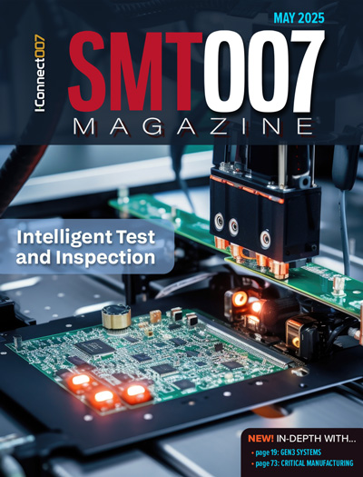
Intelligent Test and Inspection
Are you ready to explore the cutting-edge advancements shaping the electronics manufacturing industry? The May 2025 issue of SMT007 Magazine is packed with insights, innovations, and expert perspectives that you won’t want to miss.
- Articles
- Columns
- Links
- Media kit
||| MENU - smt007 Magazine
Exploring Cold Milling as an Alternative PCB Component Removal Method
January 24, 2024 | Bob Wettermann, BEST Inc.Estimated reading time: Less than a minute
When a PCB undergoes multiple heat cycles, inherent risks emerge, primarily due to the expansion and contraction of materials. This thermal stress can induce various issues, including delamination, warping, compromised solder joints, and damage to heat-sensitive components like integrated circuits or capacitors.
To counter these risks, one approach involves a unique process called "cold milling," designed to mitigate the adverse effects of additional thermal stress. Unlike traditional methods involving direct heat application, this solution utilizes a laser-guided precision mill to remove components. This ESD-safe process includes a vacuum nozzle that simultaneously removes debris during the milling process, ensuring cleanliness.
The genesis of “cold milling” stems from a customer's challenge with removing underfilled BGAs. They encountered issues with underfill leaching into the adjacent solder during reflow, causing solder shorts. By utilizing this cold milling process, we were able to remove the component without applying heat and place a new component in its place resulting in a yield >90% and a successful solution for the customer.
To read this entire article, which appeared in the January 2024 issue of SMT007 Magazine, click here.
Suggested Items
Smarter Machines Use AOI to Transform PCB Inspections
06/30/2025 | Marcy LaRont, PCB007 MagazineAs automated optical inspection (AOI) evolves from traditional end-of-process inspections to proactive, in-line solutions, the integration of AI and machine learning is revolutionizing defect reduction and enhancing yields, marking a pivotal shift in how quality is managed in manufacturing.
Magnalytix and Foresite to Host Technical Webinar on SIR Testing and Functional Reliability
06/26/2025 | MAGNALYTIXMagnalytix, in collaboration with Foresite Inc., is pleased to announce an upcoming one-hour Webinar Workshop titled “Comparing SIR IPC B-52 to Umpire 41 Functional & SIR Test Method.” This session will be held on July 24, 2025, and is open to professionals in electronics manufacturing, reliability engineering, and process development seeking insights into new testing standards for climatic reliability.
The Death of the Microsection
06/26/2025 | Bob Neves, Reliability Assessment Solutions, Inc.I got my start out of college grinding and polishing PCB microsections. My thumbs are a bit arthritic today because of the experience (microsection grinders know what I mean). Back then, via structures were rather large, and getting to the center in six steps of grinding and polishing was easy compared to what my team has been doing recently at the lab.
Specially Developed for Laser Plastic Welding from LPKF
06/25/2025 | LPKFLPKF introduces TherMoPro, a thermographic analysis system specifically developed for laser plastic welding that transforms thermal data into concrete actionable insights. Through automated capture, evaluation, and interpretation of surface temperature patterns immediately after welding, the system provides unprecedented process transparency that correlates with product joining quality and long-term product stability.
Knocking Down the Bone Pile: Tin Whisker Mitigation in Aerospace Applications, Part 3
06/25/2025 | Nash Bell -- Column: Knocking Down the Bone PileTin whiskers are slender, hair-like metallic growths that can develop on the surface of tin-plated electronic components. Typically measuring a few micrometers in diameter and growing several millimeters in length, they form through an electrochemical process influenced by environmental factors such as temperature variations, mechanical or compressive stress, and the aging of solder alloys.


