-

- News
- Books
Featured Books
- smt007 Magazine
Latest Issues
Current Issue
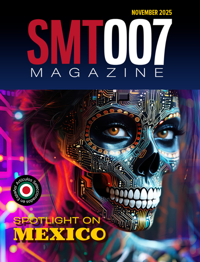
Spotlight on Mexico
Mexico isn’t just part of the electronics manufacturing conversation—it’s leading it. From growing investments to cross-border collaborations, Mexico is fast becoming the center of electronics in North America. This issue includes bilingual content, with all feature articles available in both English and Spanish.

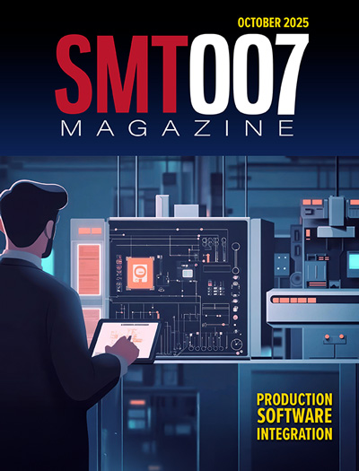
Production Software Integration
EMS companies need advanced software systems to thrive and compete. But these systems require significant effort to integrate and deploy. What is the reality, and how can we make it easier for everyone?

Spotlight on India
We invite you on a virtual tour of India’s thriving ecosystem, guided by the Global Electronics Association’s India office staff, who share their insights into the region’s growth and opportunities.
- Articles
Article Highlights
- Columns
- Links
- Media kit
||| MENU - smt007 Magazine
SMTA Announces Wafer-Level Packaging Symposium Program
January 8, 2025 | SMTAEstimated reading time: 1 minute
The SMTA is excited to announce the technical program for the 2025 Wafer-Level Packaging Symposium. The symposium will be held February 18-20, 2025 at The Hyatt Regency San Francisco Airport in San Francisco, California.
The technical program features a special keynote presentation. On Wednesday, February 19, 2025, Eric Breckenfeld, Nvidia, and Erik Hadland, Semiconductor Industry Association, will co-present, “The CHIPS and Science Act: Past, Present and Future of U.S. Microelectronics R&D.”
Technical sessions include over 20 expert speakers who delve into wafer-level packaging advances, assembly/integration process, novel interconnect & packaging process and materials, substrate/integration platform, test & metrology, fan-out wafer-level packaging, and more. The program features presentations from leading companies including adeia, Nvidia, NHanced Semiconductors, Semiconductor Industry Association, and universities such as Hanyang University, Yokohama National University, and more.
The symposium kicks off with two professional development courses on Tuesday, February 18, 2025. The first course, “Materials for Semiconductor Packaging,” will be instructed by Terry Alford, Arizona State University. Gamal Refai Ahmed, Ph.D., AMD, will instruct the second course, “Current & Future Challenges and Solutions in AI & HPC System & Thermal Management.” Access to these courses is included in standard registration.
Registration for this event is open. Click here to register. Discounted rates are available by registering on or before January 27, 2025. All presentations, professional development courses and events open to attendees are included in registration.
Testimonial
"In a year when every marketing dollar mattered, I chose to keep I-Connect007 in our 2025 plan. Their commitment to high-quality, insightful content aligns with Koh Young’s values and helps readers navigate a changing industry. "
Brent Fischthal - Koh YoungSuggested Items
Nortech Systems Incorporated Earns AS9100 Certification for Monterrey, Mexico Facility
11/04/2025 | BUSINESS WIRENortech Systems, Incorporated, a leading provider of design and manufacturing solutions for complex electromedical devices and electromechanical systems, announced that its Monterrey, Mexico, facility has achieved AS9100:D certification.
Aircraft Wire and Cable Market to surpass USD 3.2 Billion by 2034
10/30/2025 | Global Market Insights Inc.The global aircraft wire and cable market was valued at USD 1.8 billion in 2024 and is estimated to grow at a CAGR of 5.9% to reach USD 3.2 billion by 2034, according to recent report by Global Market Insights Inc.
The Training Connection Continues to Grow with Addition of Veteran IPC Trainer Bill Graver
10/30/2025 | The Training Connection LLCThe Training Connection, LLC (TTC-LLC), a premier provider of test engineering and development training, is proud to announce the addition of Bill Graver to its growing team of industry experts. A respected professional with more than 35 years in electronics manufacturing, Bill joins as an IPC Master Trainer, bringing a wealth of hands-on experience in PCB testing, failure analysis, and process improvement.
I-Connect007 Welcomes New Columnist: Leo Lambert, EPTAC
10/30/2025 | I-Connect007I-Connect007 is excited to announce a column by Leo Lambert, an industry veteran with 40 years of experience, an award winner, and technical director at EPTAC. This column, Learning With Leo, will explore the evolution and related challenges of electronics product assembly, especially as it relates to training.
On the Line With… Ultra HDI Podcast—Episode 7: “Solder Mask: Beyond the Traces,” Now Available
10/31/2025 | I-Connect007I-Connect007 is excited to announce the release of the seventh episode of its 12-part podcast series, On the Line With… American Standard Circuits: Ultra HDI. In this episode, “Solder Mask: Beyond the Traces,” host Nolan Johnson sits down with John Johnson, Director of Quality and Advanced Technology at American Standard Circuits, to explore the essential role that solder mask plays in the Ultra HDI (UHDI) manufacturing process.


