


 The Marketing Minute: Marketing With Layers
 The Right Approach: Electro-Tek—A Williams Family Legacy, Part 1
 It’s Only Common Sense: If You’re Not Differentiated, You’re Dead


Three Industry Giants From WKK Gather Around for Discussion
December 10, 2014 | Barry Matties, I-Connect007Estimated reading time: 17 minutes
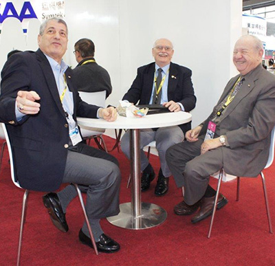
During the recent HKPCA show I had the opportunity to catch up with Hamed El-Abd, Lionel Fullwood, and Gene Weiner. Our discussion covered an array of topics, from politics to new PCB factories and what it takes to stay competitive. Below is the transcription from our conversation.
007: Here with me today is Hamed El-Abd, Lionel Fullwood and Gene Weiner from WKK, welcome guys.
GW: Barry, it’s good to see you again in China, the number one economy in the world as of this quarter.
007: Thank you, and that’s what I’ve read just this morning.
GW: And that is clearly because of numbers, not because of technology. The leading technology here is still coming in from the foreigners, including the Taiwanese, who are classed as foreigner.
007: Gene you’ve been coming to China for many years now, correct?
GW: Since 1983.
007: One of the things that strikes me is the amount of change that has happened in just the last five years in particular. What changes have you seen and what’s your opinion on it?
GW: Well with the change a lot of it is superficial. Much of it is a new younger government tightening up, and much of it is from a stronger economic position globally and a stronger military. The Chinese have put themselves in a position to be a power player, if not the power player in the world. They’re still copying, copying, copying and not paying much attention to specs. Mostly it’s homegrown products for homegrown companies, with the best technology still coming from Europe, the U.S., Japan and Taiwan. From Taiwan I would say it’s the application of the technology improvements done by ITRI, their government sponsored research, as well as their major companies.
007: In comparison to the U.S., where obviously you've spent a lot of time, what do you see happening from your point of view?
GW: The U.S. is struggling to maintain a position with a government that appears confused with economic, domestic, and foreign policies. However, quietly happening in the U.S., and not for volume but for technology, we're seeing some great advances in R&D in chips, packages, chipsets, as well as the quiet building of new automated factories in captive shops not publicly known. Lockheed has three in-house printed circuit shops and the public thinks there's only one. It’s now become an open secret that Intel is building a shop in Chandler. Two weeks ago Lionel and I visited Whelen’s new factory in New Hampshire and it’s the first fully automated new printed circuit shop in North America—and I really mean fully automated. The only things that were not part of the automation line was a separate semi-automatic layup set-up and multilayer pressing line by Burkle, an offline ENIG electroless nicke/gold and a plasma machine. Everything else was inline, automated, with a very modern design. Instead of treating the air and water of the entire building they use semiconductor techniques with tunnels around the equipment, making it easier to maintain the environment, and they didn't have to get one single permit for waste treatment because the plant is almost 100% total recycle of air, fumes, and liquid. Copper is plated out of the spent etchant, the ammonia is recaptured and put back in—it was amazing. And we were watching the first runs of 100 panel lots when we were there, and Lionel is doing some evaluation of some new imaging equipment which we can't give you the details on until perhaps spring.
007: Are they in production now?Page 1 of 3
Share on:


Testimonial
"In a year when every marketing dollar mattered, I chose to keep I-Connect007 in our 2025 plan. Their commitment to high-quality, insightful content aligns with Koh Young’s values and helps readers navigate a changing industry. "
Brent Fischthal - Koh YoungSuggested Items
Episode 6 of Ultra HDI Podcast Series Explores Copper-filled Microvias in Advanced PCB Design and Fabrication
10/15/2025 | I-Connect007I-Connect007 has released Episode 6 of its acclaimed On the Line with... American Standard Circuits: Ultra High Density Interconnect (UHDI) podcast series. In this episode, “Copper Filling of Vias,” host Nolan Johnson once again welcomes John Johnson, Director of Quality and Advanced Technology at American Standard Circuits, for a deep dive into the pros and cons of copper plating microvias—from both the fabricator’s and designer’s perspectives.
Nolan’s Notes: Tariffs, Technologies, and Optimization
10/01/2025 | Nolan Johnson -- Column: Nolan's NotesLast month, SMT007 Magazine spotlighted India, and boy, did we pick a good time to do so. Tariff and trade news involving India was breaking like a storm surge. The U.S. tariffs shifted India from one of the most favorable trade agreements to the least favorable. Electronics continue to be exempt for the time being, but lest you think that we’re free and clear because we manufacture electronics, steel and aluminum are specifically called out at the 50% tariff levels.
MacDermid Alpha & Graphic PLC Lead UK’s First Horizontal Electroless Copper Installation
09/30/2025 | MacDermid Alpha & Graphic PLCMacDermid Alpha Electronics Solutions, a leading supplier of integrated materials and chemistries to the electronics industry, is proud to support Graphic PLC, a Somacis company, with the installation of the first horizontal electroless copper metallization process in the UK.
Electrodeposited Copper Foils Market to Grow by $11.7 Billion Over 2025-2032
09/18/2025 | Globe NewswireThe global electrodeposited copper foils market is poised for dynamic growth, driven by the rising adoption in advanced electronics and renewable energy storage solutions.
MacDermid Alpha Showcases Advanced Interconnect Solutions at PCIM Asia 2025
09/18/2025 | MacDermid Alpha Electronics SolutionsMacDermid Alpha Electronic Solutions, a global leader in materials for power electronics and semiconductor assembly, will showcase its latest interconnect innovations in electronic interconnect materials at PCIM Asia 2025, held from September 24 to 26 at the Shanghai New International Expo Centre, Booth N5-E30