-

- News
- Books
Featured Books
- smt007 Magazine
Latest Issues
Current Issue
Moving Forward With Confidence
In this issue, we focus on sales and quoting, workforce training, new IPC leadership in the U.S. and Canada, the effects of tariffs, CFX standards, and much more—all designed to provide perspective as you move through the cloud bank of today's shifting economic market.

Intelligent Test and Inspection
Are you ready to explore the cutting-edge advancements shaping the electronics manufacturing industry? The May 2025 issue of SMT007 Magazine is packed with insights, innovations, and expert perspectives that you won’t want to miss.

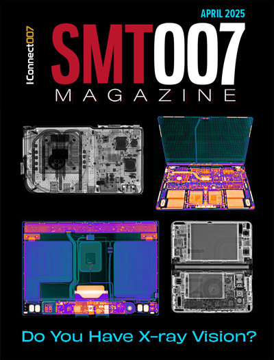
Do You Have X-ray Vision?
Has X-ray’s time finally come in electronics manufacturing? Join us in this issue of SMT007 Magazine, where we answer this question and others to bring more efficiency to your bottom line.
- Articles
- Columns
Search Console
- Links
- Media kit
||| MENU - smt007 Magazine
Bead Probe Implementation: A No-clean Case Study
December 31, 1969 |Estimated reading time: 6 minutes
By Mike Farrell, Agilent Technologies Inc. and Glen Leinbach, Caber Contacts LLC
Relying on conventional in-circuit test (ICT) pads could result in test coverage reduction in cases where density and speed requirements are demanding. A major OEM using DDR2 technology encountered this problem. To leverage the existing ICT process, the OEM conducted an experiment with bead probe technology.
High-speed busses connecting DDR2 memory devices, a DIMM connector, the controller ASIC, and other components could not accommodate conventional ICT probe pads due to signal integrity requirements and layout limitations. This meant testing the DDR2 section at functional test only, complicating component-level diagnosis and increasing repair costs in manufacturing.
On a previous board similar to this design, test access using conventional probing technology also was not able to test the DDR2 section of the board and DIMM connector. The DDR2 section of the controlling ASIC and the DDR2 memory devices were tested at functional test only. Defects were difficult and expensive to isolate. Also, pull-up and pull-down resistors and capacitors associated with the DDR2 section could not be tested at functional test. AOI, X-ray, or visual inspection alternatives were not considered in this case. The goal was to leverage the existing ICT process. The OEM decided to conduct an opportunistic experiment: implement bead probe technology 1-3 in the DDR2 section of the board to increase test access.
Board LayoutThe first step was to develop a layout component (test attribute) for the CAD design system for a bead probe test access point, while meeting the OEM's standard layout rules. The resulting geometry was an obround opening in the solder mask, providing a bead probe's test pad at 20 mils long on a 4-mil trace. Bead probe test access was implemented only on the DDR2 and USB 2.0 sections, where it was impractical to place conventional test pads (Figure 1).The final board design had 148 nodes that used bead probe test access locations. Additional test access reached two DDR2 memory devices, the DDR2 DIMM connector, associated resistors and capacitors, and the DDR2 section of the ASIC. The added 148 points increased the board's test access from 46% to 70% of total circuit nodes. Test coverage prior to adding test access to the DDR2 section was approximately 45%. This additional test access significantly improved total test coverage for the board from 45% to 85%.
The ICT FixtureHeadless, flat-faced (smooth) probes with the same diameter as the probe shaft* were used. The fixture was a dual-well vacuum box capable of testing four boards at a time. Adding top-side probing added less than $5,000 to the fixture cost. The increased test coverage outweighed the initial investment. If double-sided probing already was required for this board, the additional cost to add bead probes would have been negligible. For standard test access, 8-oz. probes were used. For bead probe locations, 6-oz. probes were used.
Fixture DebugAfter receiving the in-circuit fixture, operators tested and debugged the ICT program. They examined the bead probe locations with a microscope. The beads were well formed and flux residue was minimal. The bead probe performed well with good electrical contact (Figure 2).Debug and test of the DDR2 section of the board where bead probes were used found no noticeable differences between standard test access and bead probes. The presence of bead probes allowed direct debugging of a DDR2 digital test model and also allowed testing the DDR2 DIMM connector using vectorless test.** Functional test did not cover the DIMM connector.
Prototype BuildThe OEM's contract manufacturer (CM) moved the product to a high-volume facility offshore for the prototype builds. During the initial run, over 600 boards were built and sent to the test solution provider's facility. These boards had contact problems on the bead probe locations and on conventional test pads, indicating that a pervasive soldering problem existed across the boards. The high-volume CM may not have known about bead probes and experimentation with this board. After design updates, the bead probe testing matter was re-communicated across test provider, CM, and OEM.
The high-volume CM built the next run of prototype boards with closer attention to bead probe quality. The CM used at least two different stencils: the recommended diamond-shaped apertures for bead probe locations, and another with circular apertures. Of approximately 275 boards sent for testing, five variations existed, using different component loading options. Test engineers suspected that the two paste stencils were divided between different versions of boards. Depending on which version of board was tested, the first-pass yield for pins contact test (where pin contact integrity is verified) was between 45% and 80%. Testing on this batch transpired more smoothly and quickly. There were limited cases where a small number of bead probe locations had minimal solder, mainly around the two USB connectors. Boards that failed the pins contact test usually would pass after repeated (between 2 and 15) cycles of activating the vacuum fixture. The SMT process engineer reviewed about 10 boards from this build and found flux residue present and still posing a potential problem, although it was reduced from the previous build.
Residue ImpactFirst-pass yield at pin contact tests fell to only about 35%. The test engineer lightly rubbed the top and bottom surfaces of the boards while wearing an ESD-safe cotton glove. Upon testing, the yield for pins contact test rose to almost 100%. This indicated that the problem probably was flux residue and not the presence of a harder oxide or a fixture problem.
The lead-free solder paste was a standard formulation from a leading paste manufacturer. This manufacturer also offers the paste formulation in a version designed to "offer increased in-circuit pin test yields." For a solder paste to be compatible with in-circuit probe testing, any flux residue left on the bead probes and conventional test pads should flake away during probing or be soft enough to allow good contact. Most leading solder paste manufacturers offer similar products.
For the second run, the solder paste manufacturer's ICT-friendly formulation was used. Upon microscopic examination of boards from both batches, differences in the properties of flux residues were apparent. Boards from the second run with the "test-friendly" solder paste had residue that either was still liquid or weak and brittle when poked with the needle probe. This should provide better electrical contact.
Operators tested 108 boards with the new solder paste. Fixture construction problems resulted in three probes being off target. As a result, 50 of the boards failed probe contact test. Of the 58 boards where the probes contacted the bead probes, 100% passed the probe contact test. This demonstrates that using a solder paste formulated for pin probe testing results in excellent probe contact.
ConclusionBead probes provided significant increases in test access and test coverage to areas and components where conventional probe access on the PCB is impossible. In this case, test access grew from 46% to 70% of circuit nodes, increasing component test coverage from 45% to 85%.
The type and amount of solder flux on no-clean lead-free boards is critical to probe contact integrity. Changing to a "test-friendly" solder paste formulated for probe testing compatibility, resulted in significant improvement in probe contact results.4,5 Solder paste and flux choices are critical for successful implementation of bead probes in no-clean processes. Probe contact may be poor if a solder paste leaves hard, gummy, or waxy residues.
Detailed communication among the OEM and CM participants is imperative. The solder paste, fixture, and stencil manufacturers also require training and communication for successful bead probe implementation. Fixture construction factors such as accuracy of probe location and proper seating of the probes contribute to success as well. SMT
REFERENCES:1. M. Doraiswamy and J. J. Grealish, "Implementation of Solder-bead Probing in High Volume Manufacturing," Proceedings, International Test Conference, Paper 5.4, Santa Clara, Calif., October 2006.2. K. P. Parker, "A New Probing Technique for High-speed/High-density Printed Circuit Boards," Proceedings IEEE International Test Conference, 2004, pp 365-374.3. K. P. Parker, "Bead Probes in Practice," Proceedings IEEE International Test Conference, Paper 26.2, Austin, Texas, November 2005.4. D. Suraski and M. Parker, "Considerations for the Pin Probe Testing of No-clean Solder Paste," www.aimsolder.com.5. B. Smith, "No-clean Solder Paste Innovations," SMT, November 1999.
* Probes were developed by Everett Charles Technologies (ECT).** Testing was performed with Agilent TestJet electrical test and VTEP vectorless suite.Mike Farrell, applications engineer, Agilent Technologies Inc., may be contacted at 900 South Taft, Loveland, Colo. 80537; (970) 679-5526. Glen Leinbach, principal, Caber Contacts LLC, may be contacted at 1400 Longs Peak Drive, Fort Collins, Colo. 80524; (970) 217-1051; glen_leinbach@cabercontacts.com. Data in this article was originally presented at the IEEE International Test Conference (ITC) 2007.


