


 Learning with Leo: Drones—Meeting Demand Without Compromise
 Nolan’s Notes: Our Spotlight on North America
 Global Sourcing Spotlight: Building a Supply Chain That Bends, Not Breaks


SJIT, Solder Joint Integrity Test, To Find Latent Defects in Printed Wiring Board Assembly
April 29, 2015 | Hiroshi Yamazaki, Hioki E.E. CorporationEstimated reading time: 4 minutes
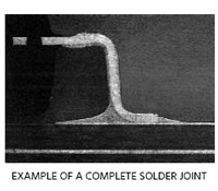
To find defects of solder joint in printed wiring board assembly, quite a few test methods have been developed so far. Capacitance method and IEEE 1149.1 or boundary scan method are often used to find opens between component leads and pads on a printed wiring board. These methods, however, can find complete opens or complete shorts only. Latent defects that can be complete defect after several years have not been found by the conversational method.
We have developed a method to find such latent defects by using 4-wire small resistance measurement technique and have built in a flying-probe in-circuit tester. It measures the resistance between component leads and pads, and checks the volume of the solder. Because the volume of the solder is inversely proportional to the resistance in-between, resistance measurement can be a way to test the solderability.
This technique is industry proven. A lot of manufacturing plants which produce printed board assembly used in automotive have adapted it. The printed wiring board assembly for automotive must endure vibration. Thus if a board assembly has a latent defect, it can bring a serious accident. In my presentation, I would like to introduce the importance of SJIT, Solder Joint Integrity Test, and a technique of SJIT.
Testing Printed Wiring Board Assembly
Printed wiring board assemblies, PWBA, are tested several times after production.The tests are categorized as production test, board-level test and system test.[1]Usually, automatic optical inspection, AOI, is done in process of production and used to not only checks component placements but also monitor the yield of the production.
The Board-level test stage follows in-process inspection at the production stage. In this stage, board assemblies are tested structurally first. Either in-circuit test or boundary-scan method or sometimes both of them are used for structural tests. The structural test, especially in-circuit test, has another purpose. It works as a pre-check for next functional test. In the functional test, power sources should be applied to the board assembly to be tested. Thus if the board assembly is not structurally complete, it can be damaged while the functional test.
The board-level structural test is done, functional tests of board-level and system-level follows.
Carrying out all the tests makes test cost increments. Thus in some cases, board-level tests are skipped and only system test is done. Moreover, in an extreme case, manufacturers do not test their products at all.
Omission of test items should be done as carefully as possible, however. It can be rebounded as a massive cost increment. Assume board-level tests including structural test and functional test are not done, and a defect is found afterwards.
Repair cost will be enormously increases as the production/test stage reaches the shipment. It is called"The 10X rule in PWBA tests."[2]
If a product including a defect comes out to the market, the problem will be much more serious.Think about the case of a car with a defective PWBA. The malfunction of the PWBA may relate to a car accident and give the driver injury. Once a defective PWBA is distributed in the market, its recall cost can be 100000X or much more.
Everyone wants to make test cost as low as possible, but as stated above, the loss will increase if test strategy is wrong. To determine test strategy, the following two factors should be considered.
1. Quality
Required degree of test quality largely depends on the quality that the products needs. A cheap complimentary toy for example does not need board-level test. If it does not work at the system level functional test, it may be thrown away.
2. Volume
How many the products is produced is another important factor to determine test strategy. For small volume production, tester may not be required, but for high volume manufacturing a dedicated tester and jigs may be required otherwise the test process can be a bottleneck.Page 1 of 2
Share on:


Testimonial
"We’re proud to call I-Connect007 a trusted partner. Their innovative approach and industry insight made our podcast collaboration a success by connecting us with the right audience and delivering real results."
Julia McCaffrey - NCAB GroupSuggested Items
BGA Technology Expands Inspection Capabilities with Creative Electron TruView X-ray System
05/08/2026 | BGA TechnologyBGA Technology, a leading provider of advanced electronics testing and inspection services, has enhanced its inspection capabilities with the addition of a Creative Electron TruView™ Simplex X-ray system at its Holbrook, New York facility.
AQUANOX A4727 and A4625 Lead KYZEN Offerings at SMTA Oregon Expo and Tech Forum
05/06/2026 | KYZENKYZEN, the global leader in innovative environmentally responsible cleaning chemistries, will exhibit at the SMTA Oregon Expo and Tech Forum scheduled to take place Thursday, May 19 at the Wingspan Event and Conference Center in Hillsboro, Oregon.
Connect the Dots: Designing for the Future of Manufacturing Reality—Surface Finish
05/07/2026 | Matt Stevenson -- Column: Connect the DotsWhen designing the complex boards that many electronic devices require to operate, designers should consider manufacturability at every step. This is my last article focused on designing for the always-evolving manufacturing reality. Choosing the right surface finish has always been important. If you are creating intricate designs with a wide variety of components, like for an ultra-high density interconnect (UHDI) board, surface finish is a critical last step.
Indium to Showcase High-Performance AI Application Solutions at SEMICON SEA 2026
05/01/2026 | Indium CorporationAs a leading provider of advanced materials solutions for today’s demanding AI applications, Indium Corporation® will feature its high-reliability product portfolio at SEMICON SEA 2026, May 5-7, in Kuala Lumpur, Malaysia.
ACCM Unveils Negative and Near-zero CTE Materials for Large-Format AI Chips
04/21/2026 | Advanced Chip and Circuit MaterialsAdvanced Chip and Circuit Materials, Inc. (ACCM) has launched two new materials: Celeritas HM50, with a negative coefficient of thermal expansion (CTE) of -8 ppm/°C to offset the positive CTE and expansion of copper with temperature on circuit boards, and Celeritas HM001, with near-zero CTE and the low-loss performance needed for high-speed signal layers to 224 Gb/s and faster in artificial intelligence (AI) circuits.