


 Smart Automation: The Journey of a Component Through an SMT Factory
 Powering the Future: Why Thermal Management Defines the Future of Electronics
 Standard of Excellence: Engineering Is the New Sales—How Technical Collaboration Wins Business


A Review of the Opportunities and Processes for Printed Electronics (Part 1)
June 22, 2015 | Happy Holden, PCB Technologist-RetiredEstimated reading time: 7 minutes

Printed electronics (PE), also called "plastic electronics," is a new and developing field of interconnect applications that is "related to PCB flexible circuit production." As microsystems continue to move towards higher speed and microminiaturization, the demands for interconnection are opening up new opportunities for "innovative" interconnects.
This article will introduce some of the technology development opportunities for PE for energy, displays, lighting, medical, sensors, information and toys. Printed electronics is focused on innovative applications at the low-end, but the needs of this market, the products already existing and the challenges of "bridging" PCBs to PE is the merging of the "printing world" and the "electronic circuits world." Solution- or liquid-based printing techniques have been utilized in the graphic arts printing industry for more than 500 years to replicate information (with pigment-based inks) on paper in high volumes and at very low costs. The application of these techniques to electronics is leading to a major paradigm shift. This has come about through the development of functional electronic materials (conductors, insulators, and semiconductors).
PE electronics are based on semiconducting, metallic conductive, nanoparticle, nanotubes and conductive organic (i.e., carbon-based) polymeric materials, usually in a solution-based format, which make it possible to deposit materials onto a surface using additive or printing techniques. Organic electronics are not about to replace the silicon in conventional chips, but there are many applications for which they have the potential offer a competitive or superior mix of novel performance and manufacturing economics.
Introduction
Printed electronics is presently an area of great interest to many in the electronics manufacturing industry. In many pieces written about printed electronics, there are projections for a myriad of potential uses for the technology and the tens of billions of dollars that are going to be made in the coming years. To those who have not been deeply involved in the electronics manufacturing industry for a long time, the term printed electronics would seem to have only entered into the industry’s lexicon since the turn of the current century, making it appear to be a new technology.
Interpreting the words printed and electronics in conjunction with one another, as a single term, one could logically assume that it means electronic circuits comprised of conductors and various active and passive components (i.e., transistors, resistors, capacitors) printed directly onto a substrate of some type. Printed electronics, according to this definition, is clearly a significant departure from traditional approaches to electronics manufacturing. However, there are a host of manufacturing solutions that marketers are trying to position under the umbrella of the new term to take advantage of the growing buzz surrounding the technology, which makes for some confusion.
According to IDTechEx, the total market for anticipated and potential printed electronics was near $2 billion in 2009 and expected to grow to nearly $60 billion within ten years. Earlier projections of a $300 billion market were floated a few years ago, but the $60 billion figure is still considerable and roughly equal to the current value of the global printed circuit market.
There is presently a market for printed electronics, but the growth rate predicted by exuberant market forecasters has not yet been seen. Barriers to exponential growth seem to be related in part to the current inability of suppliers to reduce costs to enable large scale manufacturing of printed electronics. So far, printed electronics has replaced a few existing applications, but has made little progress creating new applications outside of radio-frequency identification (RFID) and organic light-emitting diode (OLED). The latter is a true printed electronics solution that has succeeded in making a solid market presence. Other than that, no real killer app or paradigm shift technology has emerged from the current fray. The simple reality is that it is especially challenging to displace incumbent products when entirely new design solutions must be developed, understood and implemented.
Printing circuits on flexible base materials
The main attraction of printing technology for the fabrication of electronics is the possibility of preparing stacks of microstructured layers, and thereby thin-film devices, in a more simple and cost-effective way compared to conventional electronics. The possibility of implementing new or improved functionalities (e.g., mechanical flexibility) also plays a role. The selection of printing method to use is determined by requirements concerning printed layers and properties of printed materials, as well as economic and technical considerations for printed products.
Presently, printing technologies divide between sheet-based and roll-to-roll-based approaches. Sheet-based techniques, such as inkjet and screen printing, are best for low-volume, high-precision work. Gravure, offset and flexographic printing are more common for high-volume production, such as solar cells, reaching 10,000 square meters per hour (m²/h). While offset and flexographic printing are mainly used for inorganic and organic conductors (the latter also for dielectrics), gravure printing is especially suitable for quality-sensitive layers like organic semiconductors and semiconductor/dielectric-interfaces in transistors, due to high layer image registration quality. Gravure printing is also suitable for inorganic and organic conductors in terms of high resolution. Organic field-effect transistors and integrated circuits can be prepared completely using mass-printing methods.
Screen printing is appropriate for fabricating electrics and electronics on an industrial scale due to its ability to produce thick layers from paste-like materials. This method can produce conducting lines from inorganic materials (e.g., for circuit boards and antennas) and insulating and passivating layers where layer thickness is more important than high resolution. Screen printing’s 50 m²/h throughput and 100μm resolution are similar to inkjet printing. This versatile and comparatively simple method is used mainly for conductive and dielectric layers, but can also be used for organic semiconductors (e.g., for organic photovoltaic cells [OPVC], and even complete organic field-effect transistors [OFET]).Page 1 of 2
Share on:


Testimonial
"Advertising in PCB007 Magazine has been a great way to showcase our bare board testers to the right audience. The I-Connect007 team makes the process smooth and professional. We’re proud to be featured in such a trusted publication."
Klaus Koziol - atgSuggested Items
ACCM Unveils Negative and Near-zero CTE Materials for Large-Format AI Chips
04/21/2026 | Advanced Chip and Circuit MaterialsAdvanced Chip and Circuit Materials, Inc. (ACCM) has launched two new materials: Celeritas HM50, with a negative coefficient of thermal expansion (CTE) of -8 ppm/°C to offset the positive CTE and expansion of copper with temperature on circuit boards, and Celeritas HM001, with near-zero CTE and the low-loss performance needed for high-speed signal layers to 224 Gb/s and faster in artificial intelligence (AI) circuits.
SMTA Ultra HDI Symposium, Day 2: Fragile Supply Chains, Fierce Innovation
04/14/2026 | Marcy LaRont, I-Connect007The Arizona weather yielded another beautiful day as we gathered for the second day of SMTA’s annual UHDI symposium. After the first full day discussing the role of AI in business and the how-tos of implementation, Avondale Mayor Mike Pineda kicked off day two, proud to showcase his city and to declare its important place in the continued development of the West Valley, an increasingly important area for tech and manufacturing.
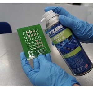
KYZEN Focuses on Aqueous and Stencil Cleaning Solutions at SMTA Monterrey Expo and Tech Forum
04/10/2026 | KYZEN'KYZEN, the global leader in innovative environmentally friendly cleaning chemistries, will exhibit at the SMTA Monterrey Expo & Tech Forum.
Solder Paste Innovations for Enhanced Reliability from MacDermid Alpha Electronics Solutions
04/10/2026 | Real Time with... APEX EXPOJason Fullerton of MacDermid Alpha Electronics Solutions discusses innovative alloys like Innolot MXE, low-temperature solder options, and polymer reinforcement strategies. Learn how these solutions address the growing demands of high-performance computing and larger component assemblies, ensuring optimal performance and cost-effectiveness.
Frank Sommer Discusses Selective Soldering Innovations for EVs
04/10/2026 | Real Time with... APEX EXPODan Beaulieu sits down with Frank Sommer, a selective soldering expert from Nordson Electronics Solutions, to discuss the resurgence of selective soldering driven by electric vehicle manufacturing, and the need for robust through-hole component integration. He also introduces Nordson's innovative SELECT Synchro selective soldering machine, designed for enhanced throughput and flexibility.