


 The Chemical Connection: Reducing Etch System Water Usage, Part 2
 It’s Only Common Sense: Nice Guys Really Can Finish First
 The Right Approach: I Hear the Train A Comin'
Physicists Fine Tune Control of Agile Exotic Materials
June 24, 2015 | UC San DiegoEstimated reading time: 2 minutes
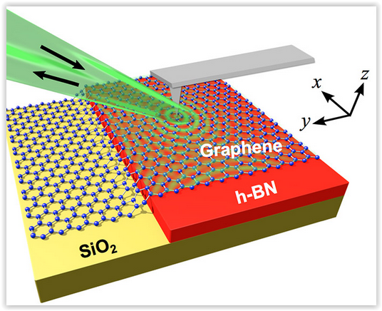
Physicists have found a way to control the length and strength of waves of atomic motion that have promising potential uses such as fine-scale imaging and the transmission of information within tight spaces.
The researchers measured waves called polaritons that can emerge when light interacts with matter. By combining two materials, they produced hybrid polaritons that propagate throughout many layers of a crystalline material and can be controlled with a simple electrical gate. The team, led by Dimitri Basov and Michael Fogler, professors of physics at the University of California, San Diego, report their success in Nature Nanotechnology.
"Our work demonstrates new properties of polaritonic waves can be achieved by artificially combining different materials," said Siyuan Dai, a graduate student in Basov's group responsible for much of the experimental work, and the lead author of the report. “The hybrid polaritons are stronger and can propagate longer and thus have greater potential in applications.”
This collaborative team was one of two to first demonstrate polaritons in single-atom layers of carbon called graphene. In graphene, infrared light launches ripples through the electrons at the surface of this metal-like material called surface plasmon polaritons that the researchers were able to control using a simple electrical circuit.
Infrared light can also launch polaritons within a different type of two-dimensional crystal called hexagonal boron nitride. Waves of atomic motion called phonon polaritons propagate throughout slabs of hBN formed by stacks of the sheetlike crystals. Basov’s and Fogler’s research groups have previously shown that varying the number of layers of hBN could control the waveform of the phonon polaritons.
Once fabricated though, a device made of hBN would confine phonon polaritons to a single narrow range of wavelengths and amplitudes.
By topping a stack of hBN with a single layer of graphene, the team has created an agile new material with hybrid polaritons that propagate throughout the crystalline slab but can be tuned with an electronic gate.
The two kind of polaritons become coupled, a theoretical consideration determined and experimental evidence confirmed. As a result, this human-made material manipulates electromagnetic radiation - light - in ways never observed in natural materials. It fits the definition of a metamaterial, a class of structures first realized at UC San Diego 15 years ago that is beginning to be expoited for potential practical use.
“Our structures are made from the new wonder material graphene and its cousin boron nitride, which endow them with several advantages compared to traditional metal-based metamaterials. The key advantages include enormous degree of tunability, relatively low losses, and ultrasmall thickness,” Fogler said.
“We have now demonstrated an entirely new class of electromagnetic metamaterials that are fabricated from separate atomic planes of van der Waals materials," Basov said. "Electromagnetic metamaterials are revolutionizing imaging and sensor technologies. Since the initial demonstration by Smith, Padilla and Schultz, these systems have already advanced to practical applications.”
Leaders in this promising field will gather for a workshop on metamaterials organized by Basov, Smith and Padilla on campus in July.
Co-authors include researchers from MIT, TU Delft, Japan's National Institute for Materials Science and Ludwig-Maximilians University. The U.S. Department of Energy, Air Force Office of Scientific Research and the Moore Foundation funded the work. F. Keilmann, a coauthor, cofounded Neaspec and Lasnix, producer of instruments used in the experiments. All other authors declare no competing financial interests.
Share on:


Suggested Items
LQDX Divests Aluminum Soldering Business - Mina™ - to Taiyo America Inc.
05/02/2024 | PRNewswireLQDX, formerly known as Averatek Corp., developer of high-performance materials for advanced semiconductor manufacturing, today announced that it has divested its aluminum soldering business – known as MinaTM – to Taiyo America Inc., a global market leader in advanced electronic materials.
Indium Corporation Expert to Present on Pb-Free Solder for Die-Attach in Discrete Power Applications
04/30/2024 | Indium CorporationIndium Corporation Product Manager – Semiconductor Dean Payne will present at the Advanced Packaging for Power Electronics conference, hosted by IMAPS, held May 8-9 in Woburn, Massachusetts, USA.
Real Time with... IPC APEX EXPO 2024: Adhesive Materials and Equipment Update with Dymax
05/01/2024 | Real Time with...IPC APEX EXPOVirginia Hogan, global business development manager at Dymax, discusses adhesive materials, dispensing and curing equipment, a new, high-reliability conformal coating, and various materials and dispensing methods.
Real Time with... IPC APEX EXPO 2024: Sustainability in the Industry
04/26/2024 | Real Time with...IPC APEX EXPOGuest Editor Henry Crandall and Chris Nash of Indium Corporation discuss the company's 90th anniversary and its focus on sustainability. They focus on the benefits of sustainable materials, their compatibility, and value propositions. The conversation also highlights how Durafuse LT technology's role in reducing reflow temperatures is leading to significant cost and energy savings. Nash also touches on downstream sustainability efforts such as using recycled materials for packaging.
SMC Korea 2024 to Highlight Semiconductor Materials Trends and Innovations on Industry’s Path to $1 Trillion
04/24/2024 | SEMIWith Korea a major consumer of semiconductor materials and advanced materials a key driver of innovation on the industry’s path to $1 trillion, industry leaders and experts will gather at SMC (Strategic Materials Conference) Korea 2024 on May 29 at the Suwon Convention Center in Gyeonggi-do, South Korea to provide insights into the latest materials developments and trends. Registration is open.