


 The Chemical Connection: Reducing Etch System Water Usage, Part 2
 It’s Only Common Sense: Nice Guys Really Can Finish First
 The Right Approach: I Hear the Train A Comin'
Large Particle Accelerator Helps Visualize Properties of Nanoscale Electronic Materials
July 17, 2015 | UCLA NewsroomEstimated reading time: 2 minutes
Scientists trying to improve the semiconductors that power our electronic devices have focused on a technology called spintronics as one especially promising area of research. Unlike conventional devices that use electrons’ charge to create power, spintronic devices use electrons’ spin. The technology is already used in computer hard drives and many other applications — and scientists believe it could eventually be used for quantum computers, a new generation of machines that use quantum mechanics to solve complex problems with extraordinary speed.
Emerging research has shown that one key to greatly improving performance in spintronics could be a class of materials called topological insulators. Unlike ordinary materials that are either insulators or conductors, topological insulators function as both simultaneously — on the inside, they are insulators but on their exteriors, they conduct electricity.
But topological insulators have certain defects that have so far limited their use in practical applications, and because they are so tiny, scientists have so far been unable to fully understand how the defects impact their functionality.
The UCLA researchers have overcome that challenge with a new method to visualize topological insulators at the nanoscale. An article highlighting the research, which was which led by Louis Bouchard, assistant professor of chemistry and biochemistry, and Dimitrios Koumoulis, a UCLA postdoctoral scholar, was published online in the Proceedings of the National Academy of Sciences.
UCLA Dimitrios Koumoulis and Louis Bouchard
The new method is the first use of beta‑detected nuclear magnetic resonance to study the effects of these defects on the properties of topological insulators.
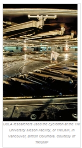
The technique involves aiming a highly focused stream of ions at the topological insulator. To generate that beam of ions, the researchers used a large particle accelerator called a cyclotron, which accelerates protons through a spiral path inside the machine and forces them to collide with a target made of the chemical element tantalum. This collision produces lithium-8 atoms, which are ionized and slowed down to a desired energy level before they are implanted in the topological insulators.
In beta‑detected nuclear magnetic resonance, ions (in this case, the ionized lithium-8 atoms) of various energies are implanted in the material of interest (the topological insulator) to generate signals from the material’s layers of interest.
Bouchard said the method is particularly well suited for probing regions near the surfaces and interfaces of different materials.
In the UCLA research, the high sensitivity of the beta‑detected nuclear magnetic resonance technique and its ability to probe materials allowed the scientists to “see” the impacts of the defects in the topological insulators by viewing the electronic and magnetic properties beneath the surface of the material.
The researchers used the large TRIUMF cyclotron in Vancouver, British Columbia.
Co-authors of the PNAS research were Danny King, formerly a UCLA graduate student in chemistry and biochemistry; Kang L. Wang, a UCLA professor of electrical engineering; Liang He, formerly a postdoctoral scholar in Wang’s lab; Xufeng Kou, formerly a graduate student in Wang’s lab; Gerald Morris and Masrur Hossain at TRIUMF; Dong Wang of the University of British Columbia; Gregory Fiete, a professor at the University of Texas, Austin; and Mercouri Kanatzidis, a professor at Northwestern University.
The research was funded by the Defense Advanced Research Project Agency’s Mesodynamic Architectures program.
Share on:


Suggested Items
LQDX Divests Aluminum Soldering Business - Mina™ - to Taiyo America Inc.
05/02/2024 | PRNewswireLQDX, formerly known as Averatek Corp., developer of high-performance materials for advanced semiconductor manufacturing, today announced that it has divested its aluminum soldering business – known as MinaTM – to Taiyo America Inc., a global market leader in advanced electronic materials.
Indium Corporation Expert to Present on Pb-Free Solder for Die-Attach in Discrete Power Applications
04/30/2024 | Indium CorporationIndium Corporation Product Manager – Semiconductor Dean Payne will present at the Advanced Packaging for Power Electronics conference, hosted by IMAPS, held May 8-9 in Woburn, Massachusetts, USA.
Real Time with... IPC APEX EXPO 2024: Adhesive Materials and Equipment Update with Dymax
05/01/2024 | Real Time with...IPC APEX EXPOVirginia Hogan, global business development manager at Dymax, discusses adhesive materials, dispensing and curing equipment, a new, high-reliability conformal coating, and various materials and dispensing methods.
Real Time with... IPC APEX EXPO 2024: Sustainability in the Industry
04/26/2024 | Real Time with...IPC APEX EXPOGuest Editor Henry Crandall and Chris Nash of Indium Corporation discuss the company's 90th anniversary and its focus on sustainability. They focus on the benefits of sustainable materials, their compatibility, and value propositions. The conversation also highlights how Durafuse LT technology's role in reducing reflow temperatures is leading to significant cost and energy savings. Nash also touches on downstream sustainability efforts such as using recycled materials for packaging.
SMC Korea 2024 to Highlight Semiconductor Materials Trends and Innovations on Industry’s Path to $1 Trillion
04/24/2024 | SEMIWith Korea a major consumer of semiconductor materials and advanced materials a key driver of innovation on the industry’s path to $1 trillion, industry leaders and experts will gather at SMC (Strategic Materials Conference) Korea 2024 on May 29 at the Suwon Convention Center in Gyeonggi-do, South Korea to provide insights into the latest materials developments and trends. Registration is open.