


 The Chemical Connection: Reducing Etch System Water Usage, Part 2
 It’s Only Common Sense: Nice Guys Really Can Finish First
 The Right Approach: I Hear the Train A Comin'
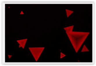
In the Realm of 2D Materials, Weirdness Works
July 23, 2015 | Pennsylvania State UniversityEstimated reading time: 6 minutes
Joshua Robinson recalls the day in 2006 when he learned of a material that is, for all practical purposes, two-dimensional.
At the time, he was a post-doctoral researcher at the Naval Research Laboratory in Washington, D.C. His advisor, Eric Snow, was raving about graphene, a newly isolated form of carbon. A cousin of the widely known buckminsterfullerene (or "buckyballs") and carbon nanotubes, graphene was a flat sheet only one carbon atom thick. The atoms were linked together in a six-sided, chicken-wire pattern, forming a lattice with astonishing properties. It was flexible, transparent, and stronger than steel. It conducted electricity better than copper and heat better than anything. In short, carbon in this form didn't behave like carbon anymore. It acted like an entirely new material.
Materials scientist Joshua Robinson looks inside a chemical vapor deposition furnace, which is used to make two-dimensional materials.
Graphene became known as the first two-dimensional, or monolayer, material. Indeed, at one-third of a billionth of a meter thick, it’s as close to two-dimensional as a tangible object can get. Graphene is 300,000 times thinner than common printer paper. If the paper was as thick as a six-story building is high, graphene would be the thickness of the original paper.
Robinson was in an ideal position to recognize the importance of two-dimensional (2D) materials. He was working with carbon nanotubes, adapting them to detect minute amounts of airborne substances such as those given off by chemical weapons and explosive devices.
“Graphene was simply an unzipped nanotube,” says Robinson, who is now an assistant professor and Corning Faculty Fellow in the Department of Materials Science and Engineering, Penn State. “Eric was so damn excited that I couldn’t help but start reading about graphene, and instantly became hooked—this ‘new material’ seemed too good to be true.”
Stumbling blocks
Scientists, engineers, and investors around the world became excited by graphene, especially its potential to revolutionize electronics. The term “post-silicon” was coined to describe this new frontier, and in 2010 the discovery and initial characterization of graphene won the Nobel Prize in Physics.
But the transition from discovery to practical application has turned out to be not so easy. Although materials scientists could create a variety of new 2D materials using other elements and compounds, they could not always predict what properties those materials would have. The tiny or even microscopic bits of monolayer were hard to manipulate and analyze—despite their strength, they were easily torn—and impossible to make on an industrial scale.
What the field needed was a deeper understanding of 2D materials and their weird properties. To take on this challenge, in 2013 Penn State’s Materials Research Institute started the Center for Two Dimensional and Layered Materials (2DLM). The center brings together about 50 faculty, postdoctoral researchers, and students from Penn State and other institutions around the country. It is the first research center to focus not just on graphene but “beyond graphene,” according to Robinson, the center’s associate director. “It has really helped attract some of the best new faculty in the nation, as well as many high-performing students.”
Inside the vapor deposition furnace, a quartz tube provides a controlled environment for the formation of 2D materials from vaporized organo-metallic compounds.
Building blocks
Work at the center addresses several broad themes, such as finding new ways to make 2D materials and combine monolayers made of different compounds, developing techniques to analyze new materials and their properties, understanding how the architecture of a layered material affects its properties, and tech transfer—seeking patents and pursuing commercially viable products.
Scientists here have made new monolayer materials by combining a variety of elements, such as tungsten or molybdenum with sulfur, gallium or silicon with selenium, and boron with nitrogen.
Improved techniques for studying 2D materials have made it easier to predict which compounds will form monolayers and how they might behave in that form. Like graphene, these materials exhibit properties not seen in their three-dimensional forms. Several of them—such as molybdenum disulfide, tungsten disulfide, and a form of boron nitride—are semiconductors that offer the promise of ultra-small electronics. Some are photoluminescent, absorbing light of one wavelength and sending the energy back out at another wavelength. They may become the basis for a new generation of devices that detect or emit light.
Some monolayer-based products are now working their way toward commercial applications.
“I have seen and touched and used flat panel displays using graphene as a conducting, transparent electrode,” says Mauricio Terrones, professor of physics, chemistry, and materials science and engineering, and director of the 2DLM. “This could be the first product in the market. The advantage of graphene is making flexible flat panels, something it is not possible to do with the current technology.”
Major projects aimed at turning such futuristic technologies into realities are under way at Penn State. The National Science Foundation (NSF) recently offered support to three of the center’s projects with more than $4 million in research grants. Robinson’s group is developing a new type of post-silicon transistor, opening the way for ever-smaller electronics. Joan Redwing, professor of materials science and engineering, and her team are working on ways to create two-dimensional materials at low temperatures, to make production more feasible for industry and to allow the materials to form on glass and plastic. Zhiwen Liu, professor of electrical engineering, and Ana Laura Elias Arriaga, research associate in physics, are working with colleagues at Rensselaer Polytechnic Institute to develop layered materials for use in light-based technologies.
Stacking monolayers
Terrones and Robinson believe that the key to success in their field will be to combine different types of monolayers. Robinson’s group has worked with other Penn State faculty and researchers at the University of Texas at Dallas to induce different two-dimensional materials to form directly on top of one another.
“By doing this, we have been able to achieve really clean interfaces between the layers,” Robinson says. “This is a key for novel nanoelectronic circuits.”
As with layered materials made of a single compound, these “hybrid” materials often display unexpected—and potentially useful—behaviors. Two such materials were made in the lab of Pulickel Ajayan, a 2DLM member at Rice University, and then sent to Terrones for analysis.
In an attempt to make the materials at lower temperatures than ever before, an advance that would ease mass production, Ajayan’s team had inadvertently caused two familiar materials to settle into new relationships with each other.
At one temperature, tungsten disulfide formed a layer on top of a layer molybdenum disulfide. In this configuration, the combined materials work like a transistor. At another temperature, the two materials formed layers side by side in the same plane.
“It is like having two different fabrics joined together, but at the joint the two fabrics are like one,” says Terrones. In the edge-to-edge configuration, the junction between the two fabrics is a meeting place where electrons and photons pass energy back and forth.
“We are now finding these materials might have important uses as very fast and sensitive photo-sensors or even light-emitting devices,” Terrones says.
A silicon wafer, shown here being inserted into a tube leading to the vapor deposition furnace, will serve as a substrate on which new 2D materials can grow.
The ‘Wild West’
With similar discoveries occurring on almost a weekly basis, predictions of amazing new products to come have returned. This time, the excitement has a sound foundation of basic science—and this time, the scientists and engineers are looking beyond the initial goal of turning graphene into a new type of semiconductor material.
“It is likely that graphene and other 2D materials will be important components of wearable electronic devices,” says Terrones. “I also foresee that we will see these materials in ‘smart’ coatings that change properties upon an external stimulus.” 2D coatings could fight rust and bacteria. They could serve as sensitive detectors of air quality. They could even discourage barnacles from fouling boat hulls. The possibilities seem limitless.
Robinson agrees.
“Two-dimensional materials are much more than a replacement for silicon,” he says. “The key thing about ‘2D’ is that it’s like the Wild West right now. There is nearly an unimaginable number of potential applications out there. But first we need to understand their basic properties to be able to best identify which applications are going to benefit from these novel materials.”
Share on:


Suggested Items
The Chemical Connection: Reducing Etch System Water Usage, Part 2
05/02/2024 | Don Ball -- Column: The Chemical ConnectionIn my last column, I reviewed some relatively simple ways to reduce water usage in existing etch systems: cutting down cooling coil water flow, adding chillers to replace plant water for cooling, lowering flow rate nozzles for rinses, etc. This month, I’ll continue with more ways to control water usage in your etcher. Most of these are not easily retrofittable to existing equipment but should be given serious consideration when new equipment is contemplated. With the right combination of add-ons, it is possible to bring the amount of water used in an etch system to almost zero.
Designer’s Notebook: What Designers Need to Know About Manufacturing, Part 2
04/24/2024 | Vern Solberg -- Column: Designer's NotebookThe printed circuit board (PCB) is the primary base element for providing the interconnect platform for mounting and electrically joining electronic components. When assessing PCB design complexity, first consider the component area and board area ratio. If the surface area for the component interface is restricted, it may justify adopting multilayer or multilayer sequential buildup (SBU) PCB fabrication to enable a more efficient sub-surface circuit interconnect.
Insulectro’s 'Storekeepers' Extend Their Welcome to Technology Village at IPC APEX EXPO
04/03/2024 | InsulectroInsulectro, the largest distributor of materials for use in the manufacture of PCBs and printed electronics, welcomes attendees to its TECHNOLOGY VILLAGE during this year’s IPC APEX EXPO at the Anaheim Convention Center, April 9-11, 2024.
ENNOVI Introduces a New Flexible Circuit Production Process for Low Voltage Connectivity in EV Battery Cell Contacting Systems
04/03/2024 | PRNewswireENNOVI, a mobility electrification solutions partner, introduces a more advanced and sustainable way of producing flexible circuits for low voltage signals in electric vehicle (EV) battery cell contacting systems.
Heavy Copper PCBs: Bridging the Gap Between Design and Fabrication, Part 1
04/01/2024 | Yash Sutariya, Saturn Electronics ServicesThey call me Sparky. This is due to my talent for getting shocked by a variety of voltages and because I cannot seem to keep my hands out of power control cabinets. While I do not have the time to throw the knife switch to the off position, that doesn’t stop me from sticking screwdrivers into the fuse boxes. In all honesty, I’m lucky to be alive. Fortunately, I also have a talent for building high-voltage heavy copper circuit boards. Since this is where I spend most of my time, I can guide you through some potential design for manufacturability (DFM) hazards you may encounter with heavy copper design.