


 The Chemical Connection: Reducing Etch System Water Usage, Part 2
 It’s Only Common Sense: Nice Guys Really Can Finish First
 The Right Approach: I Hear the Train A Comin'
UCSB Becomes West Coast Hub for National Photonics Manufacturing Institute
July 30, 2015 | UCSBEstimated reading time: 4 minutes
In a bid to boost photonics manufacturing and bring more skilled, high-tech jobs to the country, as well as push the boundaries of energy efficiency and performance in computing and telecommunications, the Obama administration announced today that it has selected the American Institute for Manufacturing of Photonics (AIM Photonics) to lead research and manufacturing of integrated photonic technology and create jobs in this important area. UC Santa Barbara is leading the West Coast division of this public-private partnership, in collaboration with the State University of New York — the lead university in this institute.
In the age of the Internet and Big Data, conventional electronic technology — even with the advent of Moore’s Law, which predicts the doubling of transistors and processing power approximately every two years — will become overwhelmed by the demand for speed, performance and data capacity.
The solution to that impending demand lies in photonics, the use of light to transmit massive amounts of data at extremely high speeds. But to make the shift between electronic wires and photonic waveguides, the two technologies must be brought together.
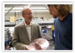
“AIM and UC Santa Barbara are leading a revolution that is integrating photonics and electronics for the benefits of both,” said John Bowers, professor of electrical and computer engineering and of materials at UCSB, director of the campus’s Institute for Energy Efficiency (IEE) and lead of the West Coast hub of AIM. Just as photonics has enabled the fiber optic communications which led to the Internet revolution, he said, the increased data capacity, speed and energy efficiency promised by photonics integrated circuits will result in enormous gains for everything from handheld devices to personal computing to data centers. “Our goal is to use complementary metal-oxide semiconductor processing to move photonics onto silicon and accelerate the integration of photonics and eliminate the data bottleneck that advanced silicon chips are facing during the next decade,” said Bowers.
“UC Santa Barbara has been a leader in integrated photonics for the past 30 years,” said UCSB Chancellor Henry T. Yang, “and this has been recognized in numerous ways, especially by three Nobel prizes: one in physics to Herb Kroemer, inventor of the double heterostructure laser, which is used in all data communications and telecom systems worldwide; one in chemistry to Alan Heeger, inventor of conductive polymers, which are widely used for displays and photovoltaic devices; and another one in physics to Shuji Nakamura, inventor of the blue LED, which is widely used for lighting.” Add to this roster of groundbreaking UCSB researchers John Bowers — considered to be one of the world’s foremost authorities in optoelectronics — whose work in the IEE seeks to provide energy efficient solutions for computing while also improving performance.
UC President Janet Napolitano said the announcement reflects how UC research advances the economic strength of both California and the nation.
“The exciting news about UC Santa Barbara serving as the West Coast hub for AIM Photonics, an Obama Administration initiative, is another testament to the value of the University of California’s research enterprise,” Napolitano said. “In this case, research by a consortium that includes our Santa Barbara, Davis, Berkeley and San Diego campuses is pushing the boundaries of energy efficiency and performance in computing and telecommunications. The research is attracting significant federal funding, as well as state and private funds, that will help create significant economic impact.”
To create a successful end-to-end integrated photonics manufacturing ecosystem in the U.S., research must be amplified, the technology supplied and a workforce trained. AIM will leverage its federal, state and private funding to expand upon already existing partnerships between research and industry to align efforts and share resources to meet the needs of this emerging industry.
With the $110 million in funding from the government, the new consortium aims to align research strength with development prowess to revitalize critical sectors of the country’s manufacturing economy. Universities, including the Massachusetts Institute of Technology, University of Arizona, Stanford University, California Institute of Technology, UC Davis, UC Berkeley, UC San Diego, Columbia University and the University of Virginia will contribute their considerable research to the consortium. Meanwhile, major integrated photonics companies such as Intel, Hewlett Packard, Infinera, Agilent, Lockheed and Raytheon as well as design software companies Synopsys, Mentor and Cadence will lead the manufacturing charge.
According to Rod Alferness, dean of the College of Engineering, UCSB already has the momentum to bring cutting-edge research and software tools for design into the manufacturing and commercial sphere. “UCSB is a worldwide leader in integrating lasers onto silicon,” he said. “Many new companies have spun out of our photonics research, including Aurrion, Agility, Calient Networks, Soraa, Aerius Photonics and Freedom Photonics.”
“Today’s announcement is a testament to the outstanding team of industrial and academic leaders assembled by AIM Photonics and its plan to establish the U.S. as a global leader in this emerging technology. Being awarded the Integrated Photonics Institute for Manufacturing Innovation (IP-IMI) would not have been possible without the critical support of Governor Andrew Cuomo, whose pioneering leadership in establishing New York State’s globally recognized, high-tech R&D ecosystem has enabled historic economic growth and innovation and secured our partnership with the state of California,” said Dr. Michael Liehr, AIM CEO and SUNY Poly Executive Vice President of Innovation and Technology and Vice President of Research. “SUNY Poly is excited to be working with partners such as UC Santa Barbara on this initiative which will be truly transformational for both the industry and the nation.”
Share on:


Suggested Items
ZESTRON Academy Launches 2024 Advanced Packaging & Power Electronics Webinar Series
05/01/2024 | ZESTRONZESTRON, the leading global provider of high-precision cleaning products, services, and training solutions in the electronics manufacturing and semiconductor industries, proudly announces the launch of its highly anticipated webinar series on Advanced Packaging & Power Electronics, a webinar series on the latest innovations, cleaning, and corrosion challenges.
NextFlex Convenes the Hybrid Electronics Community at Binghamton University
05/01/2024 | NextFlexBinghamton University hosted the NextFlex hybrid electronics community on April 18 for a day of expert presentations, breakout sessions on technology and manufacturing topics, and networking.
HQ NextPCB of HQ Electronics Debut on the International Stage for Electronics Manufacture at IPC APEX 2024
05/01/2024 | PRNewswireHQ NextPCB of HQ Electronics, a leading Chinese-based multilayer PCB manufacturer and assembly house showcased its industrial prowess on the international stage for the first time at the IPC APEX Expo 2024.
All-Inclusive: PRIDE Industries Helps Employees With Disabilities to Succeed
05/01/2024 | Sandy Gentry, IPCPRIDE Industries is the leading employer of people with disabilities and those with other barriers to employment in the United States, including veterans and former foster youth. The company offers job training, placement, on-the-job coaching, and skills development for independent living. It has held IPC membership since 2000. Read more about this unique business and its connection to the electronics manufacturing industry.
U.S. Companies Invest Heavily in Robots
04/30/2024 | IFRManufacturing companies in the United States have invested heavily in more automation: total installations of industrial robots rose by 12% and reached 44,303 units in 2023. Number one adopter is the car industry followed by the electrical and electronics sector.