


 The Chemical Connection: Reducing Etch System Water Usage, Part 2
 It’s Only Common Sense: Nice Guys Really Can Finish First
 The Right Approach: I Hear the Train A Comin'
Researchers Discover Phagraphene, a "Relative" of Graphene
September 4, 2015 | MIPTEstimated reading time: 5 minutes
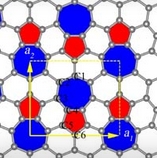
A group of scientists from Russia, the USA and China, led by Artyom Oganov from the Moscow Institute of Physics and Technology (MIPT), using computer generated simulation have predicted the existence of a new two-dimensional carbon material, a “patchwork” analogue of graphene called phagraphene. The results of their investigation were recently published in the journal Nano Letters.
“Unlike graphene, a hexagonal honeycomb structure with atoms of carbon at its junctions, phagraphene consists of penta-, hexa- and heptagonal carbon rings. Its name comes from a contraction of Penta-Hexa-heptA-graphene,” says Oganov, head of the MIPT Laboratory of Computer Design.
Two-dimensional materials, composed of a one-atom-thick layer, have attracted great attention from scientists in the last few decades. The first of these materials, graphene, was discovered in 2004 by two MIPT graduates, Andre Geim and Konstantin Novoselov. In 2010 Geim and Novoselov were awarded the Nobel Prize in physics for that achievement.
Due to its two-dimensional structure, graphene has absolutely unique properties. Most materials can transmit electric current when unbound electrons have an energy that corresponds to the conduction band of the material. When there is a gap between the range of possible electron energies, the valence band, and the range of conductivity (the so-called forbidden zone), the material acts as an insulator. When the valence band and conduction band overlap, it acts a conductor, and electrons can move under the influence of electric field.
In graphene each carbon atom has three electrons that are bound to electrons in neighboring atoms, forming chemical bonds. The fourth electron of each atom is “delocalized” throughout the whole graphene sheet, which allows it to conduct electrical current. At the same time, the forbidden zone in the graphene has zero width. If you plot the electron energy and their location in graph form, you get a figure resembling an hour glass, i.e. two cones connected by vertices. These are known as Dirac cones.
Due to this unique condition, electrons in graphene behave very strangely: all of them have one and the same velocity (which is comparable to the velocity of light), and they possess no inertia. They appear to have no mass. And, according to the theory of relativity, particles traveling at the velocity of light must behave in this manner. The velocity of electrons in graphene is about 10 thousand kilometers a second (electron velocities in a typical conductor vary from centimeters up to hundreds of meters per second).
Phagraphene, discovered by Oganov and his colleagues through the use of the USPEX algorithm, as well as graphene, is a material where Dirac cones appear, and electrons behave similar to particles without mass.
“In phagraphene, due to the different number of atoms in the rings, the Dirac cones are 'inclined.' That is why the velocity of electrons in it depends on the direction. This is not the case in graphene. It would be very interesting for future practical use to see where it will be useful to vary the electron velocity,” Artyom Oganov explains.
Phagraphene possesses all the other properties of graphene that allows it to be considered an advanced material for flexible electronic devices, transistors, solar batteries, display units and many other things.
Share on:


Suggested Items
Ansys, TSMC Enable a Multiphysics Platform for Optics and Photonics, Addressing Needs of AI, HPC Silicon Systems
04/25/2024 | PRNewswireAnsys announced a collaboration with TSMC on multiphysics software for TSMC's Compact Universal Photonic Engines (COUPE). COUPE is a cutting-edge Silicon Photonics (SiPh) integration system and Co-Packaged Optics platform that mitigates coupling loss while significantly accelerating chip-to-chip and machine-to-machine communication.
T-Global Technology Offers Solutions for Thermal Management Challenges
04/10/2024 | I-Connect007 Editorial TeamJames Hopkins from T-Global discusses the company's focus on thermal management products, including thermal interface materials, heat sinks, and thermal simulation services. He highlights the importance of collaborating with mechanical engineers and addressing challenges in balancing thermal performance and mechanical requirements. Hopkins also mentions the role of thermal simulation in guiding product recommendations and the significance of early collaboration among stakeholders for optimal product outcomes.
The Exploration Company Leverages Ansys to Promote Sustainability in Space
04/05/2024 | ANSYSSpace logistics startup The Exploration Company is advancing sustainable space exploration by leveraging Ansys simulation solutions to develop its modular and reusable space vehicle, Nyx.
Ansys Forms OEM Partnership with SynMatrix to Accelerate RF Filter Design
04/01/2024 | ANSYSAnsys announced a new OEM partnership with SynMatrix to streamline RF filter design workflows for wireless communications applications. SynMatrix develops industry-leading RF filter design and optimization tools that integrate with HFSS electromagnetic simulation.
Altair SimSolid Transforms Simulation for Electronics Industry
03/29/2024 | AltairAltair, a global leader in computational intelligence, announced the upcoming release of Altair SimSolid for electronics, bringing game-changing fast, easy, and precise multi-physics scenario exploration for electronics, from chips, PCBs, and ICs to full system design.