


 Standard of Excellence: Speed vs. Quality in Customer Service
 Knocking Down the Bone Pile: Revamp Your Components with BGA Reballing
 Global Sourcing Spotlight: Balancing Speed and Flexibility Without Sacrificing Control


ELCOSINT - The Future of High Temperature Interconnect
September 22, 2015 | Pete Starkey, I-Connect007Estimated reading time: 4 minutes
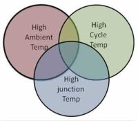
The increasing need for electronic assemblies to endure high-temperature operating conditions in aerospace, automotive, oil and gas drilling, power management and renewable energy applications, whether those conditions involve high ambient temperatures, high cycle temperatures or high junction temperatures, is driving the development of high temperature interconnection technologies. And the anticipated expiration of RoHS exemptions on the use of lead-based high melting point solder alloys justifies the exploration of alternative routes to achieving reliable interconnection whilst not departing fundamentally from established assembly process flow or processing temperatures.
The Electronic Component Sintered Interconnections (ELCOSINT) collaborative R&D project, supported by Innovate UK, set out three years ago to develop novel polymeric, sintered interconnection materials to replace high-lead-content materials and further increase the operating temperature capability of electronic assemblies to 225°C and beyond. As the project approaches its conclusion, the project partners Microsemi Semiconductor, Gwent Electronic Materials and National Physical Laboratory have presented their findings to date in a webinar moderated by Bob Willis. Microsemi Semiconductor specialises in electronics packaging and system integration for high value high reliability applications, Gwent Electronic Materials is a specialist developer of novel inks and materials for the electronics and medical diagnostic industries, and National Physical Laboratory is the UK’s national measurement institute.
Trace Wotherspoon, Senior Electronic Design Engineer at Microsemi, gave a general introduction and reviewed the project objectives: to develop a printable “solder paste like” material capable of operation at temperatures above 225°C, but processable at low temperature, and lead-free. Besides providing electrical interconnection between substrate and components, the material required adequate bond strength to support the joint at high operating temperatures throughout the life of the assembly. From a processing point of view it needed to be usable in a standard SMT assembly flow, with good shelf life and pot life. Finally, it needed to be financially competitive with established materials.
Laura Statton, Development Chemist at Gwent described the preparation of a range of conductive adhesives based on silicone resins capable of sustained high temperature operation, compounded with nano and macro silver powders and flakes, metallo-organics and solvents to produce printable pastes capable of being sintered at low temperatures. The materials had been further developed to increase screen life and stand-off height and three formulations had been supplied to Microsemi for evaluation in the building of demonstrators.
Fiona Lambert, Senior Process Engineer at Microsemi reviewed basic processing requirements: paste rheology and particle size compatible with fine-pitch stencil printing, and sufficient tackiness at room temperature to hold components in position during placement. Evaluation of initial formulations revealed issues with smearing and drying on the stencil, together with streaks and peaks on the deposit. In cooperation with Gwent, a series of systematic DOE cause-and-effect exercises with materials, solvents and print parameters resulted in improved print performance, particularly on small pad sizes. A tendency to voiding on curing was eliminated by further experimentation with printing and curing parameters. This also led to improved control of stand-off height, which had been observed to have a significant effect on joint strength. Once optimum process parameters had been established, sample assemblies passed a series of qualification tests to IPC-A-610, J-STD-020 and MIL-STD-883 for moisture sensitivity, thermal and mechanical stress. A high temperature automotive amplifier, normally assembled with high-lead solder, was built as a demonstrator product for Elcosint material.
Martin Wickham, Senior Research Scientist with the Electronic Interconnections Group at the National Physical Laboratory, discussed in detail the results of fitness-for-purpose testing. The test vehicles chosen were high-temperature resistor structures on polyimide-glass or PTFE-ceramic PCBs with ENEPIG finish, or ceramic substrates with thick-film gold finish. The component termination finish was platinum-silver. Elcosint pastes were printed using a laser-cut 75 micron stainless steel stencil with apertures of 100% or 50% of pad area and the components were auto-placed. The only departure from standard SMT practice was a batch-oven cure at 250°C for 35 minutes instead of conveyorised reflow. The assembled test vehicles were subjected to extended ageing with electrical and shear force measurements, using samples assembled with high-melting-point solder as a reference. Results were shown for ageing conditions of 7,000 hours at 85°C/85%RH, 6500 hours at temperatures of 250°C and 300°C, and 500 hours at 250°C followed by 2750 thermal cycles of -55°C to +125°C. In every case, the Elcosint materials out-performed best-in-class high-melting-point solder, maintaining a combination of low-resistance electrical continuity and good bond strength. Fourier-Transform infra-red spectroscopy offered a means of monitoring long-term resin degradation effects.
In certain of the high-melting-point soldered assemblies, some failures of copper tracks were observed, and it was believed that a contributing factor was the high peak reflow temperature - approximately 325°C - causing degradation of the structure of the printed circuit. A great benefit of the Elcosint technology was that the highest temperature seen during assembly was the 250°C cure cycle, so that the substrate and components were exposed to significantly less thermal stress. Soldering showed one physical advantage in the assembly process through its ability to self-align components by surface tension during melting and wetting. For this reason, accurate pick-and-place positioning was critical when Elcosint materials were used.
The outcome of the Elcosint project has been to produce a range of new high-temperature interconnect materials that offer a technically and commercially viable alternative to solder. The collaborative partners continue to work together in a new project named Tamessa which aims to develop an integrated system to eliminate the need to use expensive and heavy ceramic technologies in applications up to 225°C and allow the integration of bespoke through hole components
Share on:


Testimonial
"Your magazines are a great platform for people to exchange knowledge. Thank you for the work that you do."
Simon Khesin - Schmoll MaschinenSuggested Items
BTU International Earns 2025 Step-by-Step Excellence Award for Its Aqua Scrub™ Flux Management System
10/29/2025 | BTU International, Inc.BTU International, Inc., a leading supplier of advanced thermal processing equipment for the electronics manufacturing market, has been recognized with a 2025 Step-by-Step Excellence Award (SbSEA) for its Aqua Scrub™ Flux Management Technology, featured on the company’s Pyramax™ and Aurora™ reflow ovens.
On the Line With… Ultra HDI Podcast—Episode 7: “Solder Mask: Beyond the Traces,” Now Available
10/31/2025 | I-Connect007I-Connect007 is excited to announce the release of the seventh episode of its 12-part podcast series, On the Line With… American Standard Circuits: Ultra HDI. In this episode, “Solder Mask: Beyond the Traces,” host Nolan Johnson sits down with John Johnson, Director of Quality and Advanced Technology at American Standard Circuits, to explore the essential role that solder mask plays in the Ultra HDI (UHDI) manufacturing process.
Rehm Wins Mexico Technology Award for CondensoXLine with Formic Acid
10/17/2025 | Rehm Thermal SystemsModern electronics manufacturing requires technologies with high reliability. By using formic acid in convection, condensation, and contact soldering, Rehm Thermal Systems’ equipment ensures reliable, void-free solder joints — even when using flux-free solder pastes.
Indium Experts to Deliver Technical Presentations at SMTA International
10/14/2025 | Indium CorporationAs one of the leading materials providers to the power electronics assembly industry, Indium Corporation experts will share their technical insight on a wide range of innovative solder solutions at SMTA International (SMTAI), to be held October 19-23 in Rosemont, Illinois.
Knocking Down the Bone Pile: Revamp Your Components with BGA Reballing
10/14/2025 | Nash Bell -- Column: Knocking Down the Bone PileBall grid array (BGA) components evolved from pin grid array (PGA) devices, carrying over many of the same electrical benefits while introducing a more compact and efficient interconnect format. Instead of discrete leads, BGAs rely on solder balls on the underside of the package to connect to the PCB. In some advanced designs, solder balls are on both the PCB and the BGA package. In stacked configurations, such as package-on-package (PoP), these solder balls also interconnect multiple packages, enabling higher functionality in a smaller footprint.