


 The Chemical Connection: Reducing Etch System Water Usage, Part 2
 It’s Only Common Sense: Nice Guys Really Can Finish First
 The Right Approach: I Hear the Train A Comin'
Graphene as Front Contact for Silicon-perovskite Tandem Solar Cells
October 6, 2015 | HZBEstimated reading time: 2 minutes
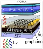
HZB team develops elegant process for coating fragile perovskite layers with graphene for the first time. Subsequent measurements show that the graphene layer is an ideal front contact in several respects.
Silicon absorbers primarily convert the red portion of the solar spectrum very effectively into electrical energy, whereas the blue portions are partially lost as heat. To reduce this loss, the silicon cell can be combined with an additional solar cell that primarily converts the blue portions. Teams at HZB have already acquired extensive experience with these kinds of tandem cells. A particularly effective complement to conventional silicon is the hybrid material called perovskite. It has a band gap of 1.6 electron volts with organic as well as inorganic components. However, it is very difficult to provide the perovskite layer with a transparent front contact. While sputter deposition of indium tin oxide (ITO) is common practice for inorganic silicon solar cells, this technique destroys the organic components of a perovskite cell.
Graphene as transparent front contact:
Now a group headed by Prof. Norbert Nickel has introduced a new solution. Dr. Marc Gluba and PhD student Felix Lang have developed a process to cover the perovskite layer evenly with graphene. Graphene consists of carbon atoms that have arranged themselves into a two-dimensional honeycomb lattice forming an extremely thin film that is highly conductive and highly transparent.
Fishing for graphene:
As a first step, the scientists promote growth of the graphene onto copper foil from a methane atmosphere at about 1000 degrees Celsius. For the subsequent steps, they stabilise the fragile layer with a polymer that protects the graphene from cracking. In the following step, Felix Lang etches away the copper foil. This enables him to transfer the protected graphene film onto the perovskite. “This is normally carried out in water. The graphene film floats on the surface and is fished out by the solar cell, so to speak. However, in this case this technique does not work, because the performance of the perovskite degrades with moisture. Therefore we had to find another liquid that does not attack perovskite, yet is as similar to water as possible”, explains Gluba.
Ideal front contact:
Subsequent measurements showed that the graphene layer is an ideal front contact in several respects. Thanks to its high transparency, none of the sunlight’s energy is lost in this layer. But the main advantage is that there are no open-circuit voltage losses, that are commonly observed for sputtered ITO layers. This increases the overall conversion efficiency. “This solution is comparatively simple and inexpensive to implement”, says Nickel. “For the first time, we have succeeded in implementing graphene in a perovskite solar cell. This enabled us to build a high-efficiency tandem device.”
Share on:


Suggested Items
The Chemical Connection: Reducing Etch System Water Usage, Part 2
05/02/2024 | Don Ball -- Column: The Chemical ConnectionIn my last column, I reviewed some relatively simple ways to reduce water usage in existing etch systems: cutting down cooling coil water flow, adding chillers to replace plant water for cooling, lowering flow rate nozzles for rinses, etc. This month, I’ll continue with more ways to control water usage in your etcher. Most of these are not easily retrofittable to existing equipment but should be given serious consideration when new equipment is contemplated. With the right combination of add-ons, it is possible to bring the amount of water used in an etch system to almost zero.
Designer’s Notebook: What Designers Need to Know About Manufacturing, Part 2
04/24/2024 | Vern Solberg -- Column: Designer's NotebookThe printed circuit board (PCB) is the primary base element for providing the interconnect platform for mounting and electrically joining electronic components. When assessing PCB design complexity, first consider the component area and board area ratio. If the surface area for the component interface is restricted, it may justify adopting multilayer or multilayer sequential buildup (SBU) PCB fabrication to enable a more efficient sub-surface circuit interconnect.
Insulectro’s 'Storekeepers' Extend Their Welcome to Technology Village at IPC APEX EXPO
04/03/2024 | InsulectroInsulectro, the largest distributor of materials for use in the manufacture of PCBs and printed electronics, welcomes attendees to its TECHNOLOGY VILLAGE during this year’s IPC APEX EXPO at the Anaheim Convention Center, April 9-11, 2024.
ENNOVI Introduces a New Flexible Circuit Production Process for Low Voltage Connectivity in EV Battery Cell Contacting Systems
04/03/2024 | PRNewswireENNOVI, a mobility electrification solutions partner, introduces a more advanced and sustainable way of producing flexible circuits for low voltage signals in electric vehicle (EV) battery cell contacting systems.
Heavy Copper PCBs: Bridging the Gap Between Design and Fabrication, Part 1
04/01/2024 | Yash Sutariya, Saturn Electronics ServicesThey call me Sparky. This is due to my talent for getting shocked by a variety of voltages and because I cannot seem to keep my hands out of power control cabinets. While I do not have the time to throw the knife switch to the off position, that doesn’t stop me from sticking screwdrivers into the fuse boxes. In all honesty, I’m lucky to be alive. Fortunately, I also have a talent for building high-voltage heavy copper circuit boards. Since this is where I spend most of my time, I can guide you through some potential design for manufacturability (DFM) hazards you may encounter with heavy copper design.