


 The Chemical Connection: Reducing Etch System Water Usage, Part 2
 It’s Only Common Sense: Nice Guys Really Can Finish First
 The Right Approach: I Hear the Train A Comin'
Graphene Key to High-density, Energy-efficient Memory Chips
October 26, 2015 | Stanford UniversityEstimated reading time: 4 minutes
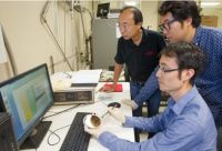
Only an atom thick, graphene is a key ingredient in three Stanford projects to create data storage technologies that use nanomaterials other than standard silicon.
The memory chips in phones, laptops and other electronic devices need to be small, fast and draw as little power as possible. For years, silicon chips have delivered on that promise.
But to dramatically extend the battery life of mobile gadgets, and to create data centers that use far less energy, engineers are developing memory chips based on new nanomaterials with capabilities that silicon can’t match.
In three recent experiments, Stanford engineers demonstrate post-silicon materials and technologies that store more data per square inch and use a fraction of the energy of today’s memory chips.
The unifying thread in all three experiments is graphene, an extraordinary material isolated a decade ago but which had, until now, relatively few practical applications in electronics.
A purified relative of pencil lead, graphene is formed when carbon atoms link together into sheets just one atom thick. Atom-thin graphene is stronger than steel, as conductive as copper and has thermal properties useful in nanoscale electronics.
“Graphene is the star of this research,” said Eric Pop, associate professor of electrical engineering and a contributor to two of the three memory projects. “With these new storage technologies, it would be conceivable to design a smartphone that could store 10 times as much data, using less battery power, than the memory we use today.”
Professor H.-S. Philip Wong and Pop led an international group of collaborators who describe three graphene-centric memory technologies in separate articles in Nature Communications, Nano Letters and Applied Physics Letters.
While consumers might appreciate the mobile application of these new technologies, engineers think post-silicon memory chips may also transform server farms that must store and deliver quick access to the vast quantities of data stored in the cloud.
“Data storage has become a significant, large-scale consumer of electricity, and new solid-state memory technologies such as these could also transform cloud computing,” Wong said.
Memory makeover
Memory chips store data as a string of ones and zeroes. Today most memory chips are based on silicon, and come in two basic types – volatile and non-volatile. Volatile memory, such as random access memory (RAM), offers fast but temporary storage. When the power shuts off, the zeros and ones vanish.
Non-volatile memory, such as the flash memory in cell phones, is slow but stable. Even if the battery expires the data remains.
The Stanford-led engineers show how to create memory with the speed of RAM and the persistence of flash by using new materials and technologies that require less energy than silicon to store the zeroes and ones.
In Nature Communications, Wong worked with postdoctoral fellow Seunghyun Lee and PhD candidate Joon Sohn on a technique known as resistive random-access memory, or RRAM for short.
In RRAM chips, tiny jolts of electricity switch certain metal oxides between resistive and conductive states. When the metal oxides resist the flow of electrons, that creates a zero. When the materials conduct electrons, that is a one. RRAM is fast, like volatile silicon memory, but like flash memory it retains stored data when the power is turned off.
This work demonstrates the possibility of constructing non-volatile RRAM while densely storing data without consuming more energy.
New phases of memory
In two other papers, published in Applied Physics Letters and Nano Letters, Pop and Wong led research teams that used graphene to make advances with a different but conceptually similar storage approach called phase-change memory.
In phase-change memory, a tiny jolt of electricity causes an alloy of germanium, antimony and tellurium to change its atomic structure. One jolt tweaks the atoms into a regular, crystalline structure that allows electrons to flow, notated as a digital one. A second jolt makes the structure irregular, or amorphous, creating a zero. Each jolt quickly toggles the phase-change material from one to zero. Like RRAM, it retains its stored data when the power is turned off.
In the Applied Physics Letters paper, Pop led a team that included former students at the University of Illinois Urbana-Champaign and collaborators at the Universities of Modena and Bologna in Italy. They used ribbons of graphene as ultra-thin electrodes to intersect phase-change memory cells, like skewers spearing marshmallows. This setup also exploited the atomically thin edge of graphene to push current into the material, and change its phase, again in an extremely energy-efficient manner.
In the Nano Letters paper, Pop and Wong used both the electrical and thermal properties of graphene in a phase-change memory chip. However, in a twist, here they used the surface of the graphene sheet to contact the phase-change memory alloy. In essence, the graphene prevented the heat from leaking out of the phase-change material, creating a more energy-efficient memory cell.
These studies show that graphene is far from a laboratory curiosity, Pop and Wong say. The material ‘s unique electrical, thermal and atomically thin properties can be utilized to create more energy-efficient data storage. Such properties do not exist in the silicon world, yet could potentially transform the way we store and access our digital data in the future.
Share on:


Suggested Items
The Chemical Connection: Reducing Etch System Water Usage, Part 2
05/02/2024 | Don Ball -- Column: The Chemical ConnectionIn my last column, I reviewed some relatively simple ways to reduce water usage in existing etch systems: cutting down cooling coil water flow, adding chillers to replace plant water for cooling, lowering flow rate nozzles for rinses, etc. This month, I’ll continue with more ways to control water usage in your etcher. Most of these are not easily retrofittable to existing equipment but should be given serious consideration when new equipment is contemplated. With the right combination of add-ons, it is possible to bring the amount of water used in an etch system to almost zero.
Designer’s Notebook: What Designers Need to Know About Manufacturing, Part 2
04/24/2024 | Vern Solberg -- Column: Designer's NotebookThe printed circuit board (PCB) is the primary base element for providing the interconnect platform for mounting and electrically joining electronic components. When assessing PCB design complexity, first consider the component area and board area ratio. If the surface area for the component interface is restricted, it may justify adopting multilayer or multilayer sequential buildup (SBU) PCB fabrication to enable a more efficient sub-surface circuit interconnect.
Insulectro’s 'Storekeepers' Extend Their Welcome to Technology Village at IPC APEX EXPO
04/03/2024 | InsulectroInsulectro, the largest distributor of materials for use in the manufacture of PCBs and printed electronics, welcomes attendees to its TECHNOLOGY VILLAGE during this year’s IPC APEX EXPO at the Anaheim Convention Center, April 9-11, 2024.
ENNOVI Introduces a New Flexible Circuit Production Process for Low Voltage Connectivity in EV Battery Cell Contacting Systems
04/03/2024 | PRNewswireENNOVI, a mobility electrification solutions partner, introduces a more advanced and sustainable way of producing flexible circuits for low voltage signals in electric vehicle (EV) battery cell contacting systems.
Heavy Copper PCBs: Bridging the Gap Between Design and Fabrication, Part 1
04/01/2024 | Yash Sutariya, Saturn Electronics ServicesThey call me Sparky. This is due to my talent for getting shocked by a variety of voltages and because I cannot seem to keep my hands out of power control cabinets. While I do not have the time to throw the knife switch to the off position, that doesn’t stop me from sticking screwdrivers into the fuse boxes. In all honesty, I’m lucky to be alive. Fortunately, I also have a talent for building high-voltage heavy copper circuit boards. Since this is where I spend most of my time, I can guide you through some potential design for manufacturability (DFM) hazards you may encounter with heavy copper design.