


 Dan’s Biz Bookshelf: ‘Abundance: How We Build a Better Future’
 Trouble in Your Tank: In Complex Systems, Design Rules Aren’t Optional
 It’s Only Common Sense: The Phone Is Still Your Competitive Advantage


Imec Advances 200mm GaN-on-Si Technology Closer to Manufacturing
December 15, 2015 | ImecEstimated reading time: 2 minutes
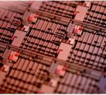
At IEEE International Electron Devices Meeting 2015, world-leading nano-electronics research center imec presented three novel aluminum gallium nitride (AlGaN)/ gallium nitride (GaN) stacks featuring optimized low dispersion buffer designs. Moreover, imec optimized the epitaxial p-GaN growth process on 200mm silicon wafers, achieving e-mode devices featuring beyond state-of-the-art high threshold voltage (Vt) and high drive current (Id).
To achieve a good, current-collapse-free device operation in AlGaN/GaN-on-Silicon (Si) devices, dispersion must be kept to a minimum. Trapped charges in the buffer between the GaN-based channel and the silicon substrate are known to be a critical factor in causing dispersion. Imec compared the impact of different types of buffers on dispersion and optimized three types: a classic step-graded buffer, a buffer with low-temperature AlN interlayers, and a super lattice buffer. These three types of buffers were optimized for low dispersion, leakage and breakdown voltage over a wide temperature range and bias conditions.
Imec also optimized the epitaxial p-GaN growth process demonstrating improved electrical performance of p-GaN HEMTs, achieving a beyond state-of-the-art combination of high threshold voltage, low on-resistance and high drive current (Vt >2V, RON= 7 Ω.mm and Id >0.4A/mm at 10V). The P-GaN HEMT results outperformed their MISHEMT counterparts.
Imec’s GaN-on-Si R&D program aims at bringing this technology towards industrialization. Imec’s offering includes a complete 200mm CMOS-compatible 200V GaN process line that features excellent specs on e-mode devices. Imec’s program allows partners early access to next-generation devices and power electronics processes, equipment and technologies, and speed up innovation at shared costs. Current R&D focuses on improving the performance and reliability of imec’s e-mode devices, while in parallel pushing the boundaries of the technology through innovation in substrate technology, higher levels of integration and exploration of novel device architectures.
“Imec’s presentations at the renowned IEDM meeting last week are a testament to the capabilities, sophistication, and maturity of our 200mm GaN-on-Silicon platform,” stated Rudi Cartuyvels, executive vice president of smart systems and energy technology at imec. “Building upon this success, we are now working with our GaN partners to implement and transfer specific device customizations. in parallel, we are exploring alternative substrate technologies to further push the boundaries of the GaN technology.”
About imec
Imec performs world-leading research in nanoelectronics. Imec leverages its scientific knowledge with the innovative power of its global partnerships in ICT, healthcare and energy. Imec delivers industry-relevant technology solutions. In a unique high-tech environment, its international top talent is committed to providing the building blocks for a better life in a sustainable society. Imec is headquartered in Leuven, Belgium, and has offices in Belgium, the Netherlands, Taiwan, USA, China, India and Japan. Its staff of about 2,300 people includes almost 700 industrial residents and guest researchers. In 2014, imec's revenue (P&L) totaled 363 million euro.
Share on:


Subscribe
Stay ahead of the technologies shaping the future of electronics with our latest newsletter, Advanced Electronics Packaging Digest. Get expert insights on advanced packaging, materials, and system-level innovation, delivered straight to your inbox.
Subscribe now to stay informed, competitive, and connected.
Suggested Items
Sony Semiconductor Solutions, TSMC Enter Preliminary Agreement for Next-Generation Image Sensor Strategic Partnership
05/08/2026 | TSMCSony Semiconductor Solutions Corporation and TSMC announced the signing of a non-binding memorandum of understanding (MOU) to form a strategic partnership for the development and manufacturing of next-generation image sensors.
BGA Technology Expands Inspection Capabilities with Creative Electron TruView X-ray System
05/08/2026 | BGA TechnologyBGA Technology, a leading provider of advanced electronics testing and inspection services, has enhanced its inspection capabilities with the addition of a Creative Electron TruView™ Simplex X-ray system at its Holbrook, New York facility.
Molex Completes Acquisition of Teramount Ltd.
05/07/2026 | PRNewswireMolex, a global electronics leader and connectivity innovator, has completed the acquisition of Teramount Ltd., an Israel‑based developer of detachable fiber‑to‑chip connectivity solutions optimized for high‑volume Co‑Packaged Optics (CPO) and other silicon photonics applications.
IBM, Aramco Explore Collaboration to Accelerate AI and Innovation Across Saudi Arabia
05/07/2026 | IBMAramco and IBM announced their intended collaboration on opportunities to advance artificial intelligence, agentic AI, automation, material science and other mutually agreed domains in the industrial sector.
Foxconn Launches Second-Gen LEO Satellite, Begins Inter-Satellite Link Testing
05/05/2026 | FoxconnFoxconn Technology Group, the world's largest electronics manufacturing services provider, announced that its second-generation low-Earth orbit (LEO) satellites, "Pearl-1A" and "Pearl-1B," were successfully launched into their designated orbits via SpaceX's Falcon 9 rocket on the evening of May 3 (Taipei time).