


 The Chemical Connection: Reducing Etch System Water Usage, Part 2
 It’s Only Common Sense: Nice Guys Really Can Finish First
 The Right Approach: I Hear the Train A Comin'
Visualizing Atoms of Perovskite Crystals
January 10, 2016 | Okinawa Institute of Science and Technology (OIST) Graduate UniversityEstimated reading time: 2 minutes
Organic-inorganic perovskite materials are key components of the new generation of solar cells. Understanding properties of these materials is important for improving lifetime and quality of solar cells. Researchers from the Energy Materials and Surface Sciences (EMSS) Unit, led by Prof. Yabing Qi, at the Okinawa Institute of Science and Technology Graduate University (OIST) in collaboration with Prof. Youyong Li's group from Soochow University (China) and Prof. Nam-Gyu Park's group from Sungkyunkwan University (Korea) report in the Journal of the American Chemical Society the first atomic resolution study of organic-inorganic perovskite.
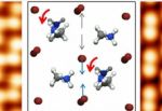
Perovskites are a class of materials with the general chemical formula ABX3. A and B are positive ions bound by negative ions X. Organic-inorganic perovskites used in solar cells are usually methylammonium lead halides (CH3NH3PbX3, where X is bromine, iodine, or chlorine). The OIST scientists used a single crystal of methylammonium lead bromide (CH3NH3PbBr3) to create topographic images of its surface with a scanning tunneling microscope.
This microscope uses a conducting tip that moves across the surface in a manner very similar to a finger moving across a Braille sign. While the bumps in Braille signs are a few millimetres apart, the microscope detects bumps that are more than million times smaller -- atoms and molecules. This is achieved by the quantum tunneling effect -- the ability of an electron to pass through a barrier. The probability of an electron passing between the material surface and the tip depends on the distance between the two. The resulting atomic-resolution topographic images reveal positions and orientations of atoms and molecules, and also provide a detailed look at structural defects in the surface.
"At room temperature atoms and molecules are quite mobile, so we decided to freeze the crystal to almost absolute zero (-269ºC) to get a good picture of its atomic structure," says Dr Robin Ohmann, a member of the EMSS Unit and the first author of the paper. The crystal was cut and studied in a vacuum to avoid contamination of the surface. Dr Ohmann's colleagues from Soochow University calculated atomic structures using principles of quantum physics and then compared them with scanning tunneling microscopy data.
Page 1 of 2
Share on:


Suggested Items
LQDX Divests Aluminum Soldering Business - Mina™ - to Taiyo America Inc.
05/02/2024 | PRNewswireLQDX, formerly known as Averatek Corp., developer of high-performance materials for advanced semiconductor manufacturing, today announced that it has divested its aluminum soldering business – known as MinaTM – to Taiyo America Inc., a global market leader in advanced electronic materials.
Indium Corporation Expert to Present on Pb-Free Solder for Die-Attach in Discrete Power Applications
04/30/2024 | Indium CorporationIndium Corporation Product Manager – Semiconductor Dean Payne will present at the Advanced Packaging for Power Electronics conference, hosted by IMAPS, held May 8-9 in Woburn, Massachusetts, USA.
Real Time with... IPC APEX EXPO 2024: Adhesive Materials and Equipment Update with Dymax
05/01/2024 | Real Time with...IPC APEX EXPOVirginia Hogan, global business development manager at Dymax, discusses adhesive materials, dispensing and curing equipment, a new, high-reliability conformal coating, and various materials and dispensing methods.
Real Time with... IPC APEX EXPO 2024: Sustainability in the Industry
04/26/2024 | Real Time with...IPC APEX EXPOGuest Editor Henry Crandall and Chris Nash of Indium Corporation discuss the company's 90th anniversary and its focus on sustainability. They focus on the benefits of sustainable materials, their compatibility, and value propositions. The conversation also highlights how Durafuse LT technology's role in reducing reflow temperatures is leading to significant cost and energy savings. Nash also touches on downstream sustainability efforts such as using recycled materials for packaging.
SMC Korea 2024 to Highlight Semiconductor Materials Trends and Innovations on Industry’s Path to $1 Trillion
04/24/2024 | SEMIWith Korea a major consumer of semiconductor materials and advanced materials a key driver of innovation on the industry’s path to $1 trillion, industry leaders and experts will gather at SMC (Strategic Materials Conference) Korea 2024 on May 29 at the Suwon Convention Center in Gyeonggi-do, South Korea to provide insights into the latest materials developments and trends. Registration is open.