


 Dan’s Biz Bookshelf: ‘The Next RenAIssance: AI and the Expansion of Human Potential’
 The Chemical Connection: When the Industry Moves Faster Than the Standards
 Driving Innovation: Selecting the Right Laser Source


Nanosheet Growth Technique Could Revolutionize Nanomaterial Production
February 1, 2016 | University of Wisconsin-MadisonEstimated reading time: 2 minutes
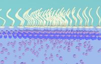
After six years of painstaking effort, a group of University of Wisconsin-Madison materials scientists believe the tiny sheets of the semiconductor zinc oxide they're growing could have huge implications for the future of a host of electronic and biomedical devices.
The group -- led by Xudong Wang, a UW-Madison professor of materials science and engineering, and postdoctoral researcher Fei Wang -- has developed a technique for creating nearly two-dimensional sheets of compounds that do not naturally form such thin materials. It is the first time such a technique has been successful.
Essentially the microscopic equivalent of a single sheet of paper, a 2-D nanosheet is a material just a few atoms thick. Nanomaterials have unique electronic and chemical properties compared to identically composed materials at larger, conventional scales.
"What's nice with a 2-D nanomaterial is that because it's a sheet, it's much easier for us to manipulate compared to other types of nanomaterials," says Xudong Wang.
Until now, materials scientists were limited to working with naturally occurring 2-D nanosheets. These natural 2-D structures include graphene, a single layer of graphite, and a limited number of other compounds.
Developing a reliable method to synthesize and manufacture 2-D nanosheets from other materials has been a goal of materials researchers and the nanotechnology industry for years.
In their technique, the UW-Madison team applied a specially formulated surfactant -- a detergent-like substance -- onto the surface of a liquid containing zinc ions.
Due to its chemical properties, the surfactant assembles itself into a single layer at the surface of the liquid, with negatively charged sulfate ions pointed in the direction of the liquid. Those sulfate ions draw the positively charged zinc ions from within the liquid to the surface, and within a couple hours enough zinc ions are drawn up to form continuous zinc oxide nanosheets only a few atomic layers thick.
Xudong Wang first had the idea for using a surfactant to grow nanosheets during a lecture he was giving in a course on nanotechnology in 2009.
"The course includes a lecture about self-assembly of monolayers," he says. "Under the correct conditions, a surfactant will self-assemble to form a monolayer. This is a well-known process that I teach in class. So while teaching this, I wondered why we wouldn't be able to reverse this method and use the surfactant monolayer first to grow the crystalline face."
After five years of trial and error with different surfactant solutions, the idea paid off.
"We are very excited about this," says Xudong Wang. "This is definitely a new way to fabricate 2-D nanosheets, and it has great potential for different materials and for many different applications."
Already, the researchers have found that the 2-D zinc oxide nanosheets they've grown are able to function as semiconductor transistors called a p-type, the opposite electronic behavior of naturally occurring zinc oxide. Researchers have for some time attempted to produce zinc oxide with reliable p-type semiconductor properties.
Zinc oxide is a very useful component of electronic materials, and the new nanosheets have potential for use in sensors, transducers and optical devices.
But the zinc oxide nanosheets are only the first of what could be a revolution in 2-D nanomaterials. Already, the UW-Madison team is applying its surfactant method to growing 2-D nanosheets of gold and palladium, and the technique holds promise for growing nanosheets from all sorts of metals that wouldn't form them naturally.
"It brings a lot of new functional material to this 2-D material category," Wang says.
Share on:


Subscribe
Stay ahead of the technologies shaping the future of electronics with our latest newsletter, Advanced Electronics Packaging Digest. Get expert insights on advanced packaging, materials, and system-level innovation, delivered straight to your inbox.Subscribe now to stay informed, competitive, and connected.
Suggested Items
I-Connect007 Editor’s Choice: Five Must-Reads for the Week
05/01/2026 | Michelle Te, I-Connect007If it feels like the PCB industry is accelerating faster than ever, you’re not imagining it. From advanced materials driven by AI applications to renewed investment in domestic manufacturing—and the next generation stepping into critical roles—there’s a lot shifting at once. My selections for this week highlight where the pressure points are forming, and where the opportunities are emerging.
Electronics Manufacturing Needs Your Voice: Global Sentiment Survey Now Live
04/30/2026 | Global Electronics AssociationThe latest monthly Global Sentiment Survey from the Global Electronics Association is now open. At a time when demand uncertainty, policy shifts, energy costs, and supply chain recalibration are pulling the industry in multiple directions, the survey captures something macroeconomic data often misses: how manufacturers are actually experiencing conditions on the ground.
From Backbone to Breakthroughs: I-Connect007 Wraps PCB Materials Series with Focus on Innovation
04/30/2026 | I-Connect007I-Connect007 wraps up its six-part podcast series, PCB Materials: The Backbone and Future of Electronics, with Episode 6 and a discussion focusing on innovation. In Episode 6, Marcy LaRont speaks with Isola CTO Kirk Thompson about a critical turning point for the PCB industry as innovation accelerates. As data rates climb and demands from AI infrastructure, power density, flexible electronics, photonics, and chiplet integration intensify, traditional material assumptions are no longer sufficient.
Jiva Soluboard Getting the Attention It Deserves
04/30/2026 | Marcy LaRont, I-Connect007 MagazineJiva is a newer company that bridges the divide between PCB fabrication and product circularity or sustainability. Jiva Soluboard is the first fully recyclable laminate material ever created for PCB fabrication, and it's not going unnoticed. Stephen Driver, CEO of Jiva, gave us an update at APEX EXPO, including an exciting certification achievement in February.
Driving Innovation: Selecting the Right Laser Source
04/28/2026 | Simon Khesin -- Column: Driving InnovationWhen I first joined Schmoll Maschinen, I brought experience from almost every PCB process, except for laser. As I immersed myself in laser processing, I realized why it can seem so daunting to a newcomer. The complexity arises from three intersecting factors: A vast variety of laser sources: CO2, UV-nano, green-pico, UV-pico, IR-pico, and others; a diverse range of applications: Drilling, cutting, ablation, and more; and an extensive list of materials: These have vastly different absorption rates. Choosing the right machine or laser source is rarely trivial. Even for experienced engineers, answering "Which source is best?" requires examining the business's specific goals.