


 Dan’s Biz Bookshelf: ‘The Next RenAIssance: AI and the Expansion of Human Potential’
 The Chemical Connection: When the Industry Moves Faster Than the Standards
 Driving Innovation: Selecting the Right Laser Source


Organic Crystals Allow Creating Flexible Electronic Devices
February 3, 2016 | Lomonosov Moscow State UniversityEstimated reading time: 3 minutes
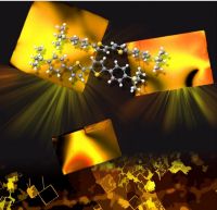
Scientists from the Faculty of Physics of the Moscow State University have grown organic semiconductor crystals which can reduce the cost of the process of creating light, flexible and transparent light-emitting electronic devices of the new generation.
A team of researchers from the Faculty of Physics of Moscow State University in cooperation with Russian and foreign colleagues learnt to grow organic semiconductor crystals with extremely high light-emitting efficiency that promise a bright future for wet-processed organic optoelectronics.
Moreover, they made a double breakthrough using much simpler and cheaper technologies that previously were considered impractical. The scientists have published the results of their work in the latest issue of the Applied Materials and Interfaces journal.
The organic optoelectronics is a rapidly growing area that promises to achieve the ultimate dream to make light, flexible and transparent electronic devices of the new generation, such as organic light-emitting transistors (OLET) and organic lasers pumped by electric current. This is, indeed, a very promising area: the organic semiconductors due to their availability can even replace silicon in some electronic applications.
It was believed that the organic semiconductor crystals grown from the vapor phase are much preferred than the ones grown from solution, since those obtained from vapor are purer and free of structure impurities. A group of physicists from the Moscow State University, led by Professor Dmitry Paraschuk, are of those who do not share this opinion, and prefer the solution growing for several reasons, particularly because of much simpler and cheaper technologies stemming from this method.
In their study, so called thiophene-phenylene oligomers were chosen as work-horse molecules. The desired molecules were synthesized for them by chemists from the Moscow State University and the Enikolopov Institute of Synthetic Polymeric Materials of RAS. At the Faculty of Physics of the Moscow State University crystals were grown from solution of these molecules. Their luminescent and electrical properties were measured there as well.
The main results of this study were overwhelming: the solution-grown crystals are more luminescent than their analogues obtained from vapor. Their quantum yield (i.e. the ratio of the number of photons emitted to the number of absorbed ones) reached 60%, whereas vapor-grown crystals presented no more than 38%.
Such a striking difference in the luminescence efficiency is explained, particularly, by the fact that, perhaps, during the solution-growing some internal radiationless channels that take some part of the excitation energy are suppressed in crystals. But, apparently, this is not the only explanation.
"We have found reasons for such a high quantum yield, but we are not ready to publish these yet. This is a matter of our future studies, "- told Professor Paraschuk.
It is noteworthy that despite all previously known disadvantages of the solution-growing techniques, the new study made it possible to talk about their advantages compared to the vapor-growing methods of crystals. In one of the recent researches, the group of Paraschuk found out that crystals can be grown on the surface of the solution instead of a solid substrate, due to the surface tension forces.
"We have shown that it is possible to grow crystals on the surface of the liquid in different ways. Roughly speaking, after we place a solution with molecules in a vessel and then begin to cool it, under some certain conditions we allow molecules to be deposited on the surface at the "air-liquid" interface. Because the liquid surface is almost perfect, the crystals grown on it are of good quality, and owing to their high electronic performance they are much more preferable to the vapor-grown ones. Moreover, the surface of the solution-grown crystals is molecularly smooth with angstrom-scale roughness, which allows us to create field-effect transistors on their basis, and its quality is irreplaceable in this case" - says the professor.
Dmitry Paraschuk emphasizes that the applicability of the crystals in light-emitted transistors, and therefore in organic optoelectronics is just a suggestion, the validity of which is still to be proved. The same situation is with the possibility of creating lasers controlled by electric current obtained on the same basis.
"People dream to get lasers that can ignite by simple connection of the film to the power source, but they haven't achieved success yet,"- told Paraschuk. - "We hope that with the help of organic crystals we can reach this goal. The combination of good conductivity and high efficiency allows us to hope that the first electrically pumped laser will be created on the basis of such crystals."
Share on:


Subscribe
Stay ahead of the technologies shaping the future of electronics with our latest newsletter, Advanced Electronics Packaging Digest. Get expert insights on advanced packaging, materials, and system-level innovation, delivered straight to your inbox.Subscribe now to stay informed, competitive, and connected.
Suggested Items
Elsyca Acquires Hivelix to Strengthen Simulation Platform for Electrochemical Surface Engineering
04/03/2026 | ElsycaElsyca, a global pioneer in computer-aided engineering (CAE) simulation for electrochemical processes and surface finishing, announces the acquisition of Hivelix, a specialist in advanced surface treatment simulation with strong expertise in multiphysics modelling and AI-assisted process optimisation.
Connect the Dots: Designing for the Future of Manufacturing Reality—Solder Mask and Legend
04/09/2026 | Matt Stevenson -- Column: Connect the DotsPCBs seem to be getting more complex by the day, so it is important for designers to keep educating themselves about the realities of manufacturing increasingly intricate boards. Last month’s column highlighted design considerations for the strip-etch-strip process and how manufacturers approach that phase of production. Now that we have a functioning board, we must protect the PCB from environmental hazards and document the circuit components. This article will detail the solder mask and legend process and offer best practices for designers to ensure a high-quality result.
Take the Mic: Photo Chemical Systems: 50 Years Strong
04/03/2026 | Real Time with... APEX EXPOPhoto Chemical Systems is celebrating 50 years in the bare board PCB market. David Graves and Jason Averette discuss how they've expanded into assembly, leveraging strong relationships and a customer-centric approach to navigate supply chain challenges. With innovative solutions and future growth strategies, including AI integration and new market ventures, Photo Chemical Systems continues enduring success.
Bold Laser Automation Introduces Precision Laser Cleaning System for Advanced Manufacturing
03/27/2026 | PRNewswireBold Laser Automation, Inc. has introduced the LPCl1820UV Laser Precision Cleaning System, a Class 1, industrial laser platform engineered for high-precision surface cleaning and thin-film removal in demanding manufacturing environments.
The Chemical Connection: Managing Cumulative Process Variations for Fun and Profit
03/23/2026 | Don Ball -- Column: The Chemical ConnectionTolerances have become increasingly tight as PCBs have grown more complex and reduced in size, weight, and power consumption. Even if we maintain a traditional ±10% variation in etched line width, the tolerance in a 50 µm (0.002" or 2 mils) wide etched line is only 5 µm (0.0002” or 0.2 mils). That’s not very much, and it gets even worse as the line and space requirements drop to 25 µm lines and spaces.