


 Happy’s Tech Talk #28: The Power Mesh Architecture for PCBs
 It’s Only Common Sense: Would You Join Your Own Company?
 The Chemical Connection: Reducing Etch System Water Usage, Part 2
Researchers Stack the Odds for Novel Optoelectronic 2D Materials
March 3, 2016 | ORNLEstimated reading time: 4 minutes
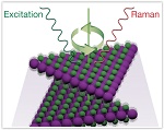
Stacking layers of nanometer-thin semiconducting materials at different angles is a new approach to designing the next generation of energy-efficient transistors and solar cells. The atoms in each layer are arranged in hexagonal arrays. When two layers are stacked and rotated, atoms from one layer overlap with those in the other layer and can form an infinite number of overlapping patterns, like the Moiré patternsthat result when two screens are overlaid and one is rotated on top of the other. Theoretical calculations predict excellent electronic and optical properties for some stacking patterns, but practically, how can these patterns be made and characterized?
Recently a team led by researchers from the Department of Energy’s Oak Ridge National Laboratory used the vibrations between two layers to decipher their stacking patterns. The team employed a method called low-frequency Raman spectroscopy to measure how the layers vibrate with respect to each other and compared the frequencies of the measured vibrations with their theoretically predicted values. Their study provides a platform for engineering two-dimensional (2D) materials with optical and electronic properties that strongly depend on stacking configurations. The findings are published in ACS Nano,a journal of the American Chemical Society.
“Low-frequency Raman spectroscopy, in combination with first-principles modeling, offers a quick and easy approach to reveal complex stacking configurations in the twisted bilayers of a promising semiconductor, without relying on other expensive and time-consuming experimental techniques,” said co-lead author Liangbo Liang, a Wigner Fellow at ORNL. “We are the first to show that low-frequency Raman spectra can be used as fingerprints to characterize the relative layer stacking in semiconducting 2D materials.”
In Raman scattering, an optical method for probing atomic vibrations, a material scatters monochromatic light from a laser. Whereas conventional Raman spectroscopy may probe more than approximately 3 trillion atomic vibrations per second, low-frequency Raman spectroscopy detects vibrations that are an order of magnitude slower. The low-frequency technique is sensitive to weak attractive forces between layers, called van der Waals coupling. It can provide crucial insight about layer thickness and stacking—aspects that govern fundamental properties of 2D materials.
“This work combines state-of-the art synthesis and processing of 2D materials, their unique spectroscopic characterization, and data interpretation using first-principles theory,” said co-lead author Alex Puretzky. “High-resolution Raman spectroscopy that can probe low-frequency modes requires specialized instrumentation, and only a few places around the world have such a capability together with advanced synthesis and characterization tools, and theory and computational modeling expertise. The Center for Nanophase Materials Sciences at ORNL is among them.”
Page 1 of 2
Share on:


Suggested Items
IDTechEx Discusses Low-Loss Materials: The Enabler of Future Connected Vehicles?
05/06/2024 | IDTechExFuture connected vehicles will offer future drivers a safer, smoother, and more convenient driving experience. Not only will drivers get access to more navigation and entertainment options, but they will also gain access to safety technologies that will potentially reduce accidents, improve congestion, and reduce emissions globally by allowing vehicle safety systems to communicate with each other and with city traffic infrastructure.
LQDX Divests Aluminum Soldering Business - Mina™ - to Taiyo America Inc.
05/02/2024 | PRNewswireLQDX, formerly known as Averatek Corp., developer of high-performance materials for advanced semiconductor manufacturing, today announced that it has divested its aluminum soldering business – known as MinaTM – to Taiyo America Inc., a global market leader in advanced electronic materials.
Indium Corporation Expert to Present on Pb-Free Solder for Die-Attach in Discrete Power Applications
04/30/2024 | Indium CorporationIndium Corporation Product Manager – Semiconductor Dean Payne will present at the Advanced Packaging for Power Electronics conference, hosted by IMAPS, held May 8-9 in Woburn, Massachusetts, USA.
Real Time with... IPC APEX EXPO 2024: Adhesive Materials and Equipment Update with Dymax
05/01/2024 | Real Time with...IPC APEX EXPOVirginia Hogan, global business development manager at Dymax, discusses adhesive materials, dispensing and curing equipment, a new, high-reliability conformal coating, and various materials and dispensing methods.
Real Time with... IPC APEX EXPO 2024: Sustainability in the Industry
04/26/2024 | Real Time with...IPC APEX EXPOGuest Editor Henry Crandall and Chris Nash of Indium Corporation discuss the company's 90th anniversary and its focus on sustainability. They focus on the benefits of sustainable materials, their compatibility, and value propositions. The conversation also highlights how Durafuse LT technology's role in reducing reflow temperatures is leading to significant cost and energy savings. Nash also touches on downstream sustainability efforts such as using recycled materials for packaging.