


 American Made Advocacy: What About the Rest of the Technology Stack?
 It’s Only Common Sense: Great Ideas From John Mitchell’s Book on Hiring Habits
 Punching Out: Breaking Out of the Valuation Box
Nanotechnologists at UT Make Orientation of Magnetism Adjustable in New Materials
March 8, 2016 | University of TwenteEstimated reading time: 2 minutes
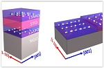
Nanotechnologists at the UT research institute MESA+ are now able to create materials in which they can influence and precisely control the orientation of the magnetism at will. An interlayer just 0.4 nanometres thick is the key to this success. The materials present a range of interesting possibilities, such as a new way of creating computer memory as well as spintronics applications – a new form of electronics that works on the basis of magnetism instead of electricity. The research was published today in the leading scientific journal Nature Materials.
Nanotechnologists at the University of Twente are specialized in creating new materials. Thanks to the top-level facilities at the MESA+ NanoLab they are able to combine materials as they wish, with the ability to control the material composition down to atom level. In particular, they specialize in creating materials composed of extremely thin layers, sometimes just one atom thick.
Computer memory
In research published today in the scientific journal Nature Materials, they show their ability to create new materials within which they can precisely and locally control the orientation of the magnetism. This opens the way to new possibilities of creating computer memory. Moreover, this method of creating materials is interesting for spintronics, a new form of electronics that does not utilize the movement of charges but instead the magnetic properties of a material. This not only makes electronics very fast and efficient, but also allows them to be produced in extremely small dimensions.
Interlayer
In the course of this research the scientists stacked up various thin layers of Perovskite materials. By placing an extremely thin interlayer of just 0.4 nanometres between the layers (a nanometre is a million times smaller than a millimetre), it becomes possible to influence the orientation of the magnetism in the individual Perovskite layers as desired, whereby the orientation of the magnetism in the bottom layer, for instance, is perpendicular to that of the layer above. By varying the location where the interlayer is applied, it becomes possible to select the local orientation of the magnetism anywhere in the material. This is an essential property for new forms of computer memory and for spintronics applications. This effect was already known for much thicker layers, but never before had researchers demonstrated that the orientation of the magnetism can be controlled so precisely with extremely thin layers, too.
Research
The research has been conducted by scientists of the MESA+ research group Inorganic Materials Science in collaboration with colleagues from other institutes, including the University of Antwerp (Belgium), the University of British Columbia (Canada) and TU Wien (Vienna, Austria). Within the research project, the Twente-based researchers were responsible for coordination and for creating the materials. The colleague researchers from Antwerp visualized the materials and were able to image even the smallest atoms in the material. The Canadian researchers created a magnetic cross-section of the material, while the Austrian researchers handled the theoretical calculations.
Share on:


Suggested Items
The Shaughnessy Report: Unlock Your High-speed Material Constraints
05/15/2024 | Andy Shaughnessy -- Column: The Shaughnessy ReportThe world of PCB materials used to be a fairly simple one. It was divided into two groups: the “traditional” laminates, often called FR-4, and the high-speed laminates developed especially for high-speed PCBs. These were two worlds that usually didn’t collide. But then traditional laminates started getting better, and high-speed designers and design engineers took notice and started to reconsider what FR-4 could be used for.
Breaking High-speed Material Constraints: Design007 Magazine — May 2024
05/14/2024 | I-Connect007 Editorial TeamDo you need specialty materials for your high-speed designs? Maybe not. Improvements in resins mean designers of high-speed boards can sometimes use traditional laminate systems instead of high-speed materials, saving time and money while streamlining the fab process. In the May 2024 issue of Design007 Magazine, our contributors explain how to avoid overconstraining your materials when working with high-speed boards.
Indium Experts to Present at Electronics in Harsh Environments SMTA Conference
05/13/2024 | Indium Corporationndium Corporation Technical Manager for Europe, Africa, and the Middle East, Karthik Vijay, will deliver a technical presentation and Indium Corporation Senior Technologist, Dr. Ronald Lasky, will deliver both a workshop and technical presentation at the Electronics in Harsh Environments SMTA Conference on May 14-16 in Copenhagen, Denmark.
Ansys’ Collaboration with Schrödinger will Accelerate Materials Development with Unprecedented Multiscale Simulation
05/09/2024 | ANSYSAnsys and Schrödinger are collaborating to deliver an ICME approach that bridges the gap between materials discovery and product development.
2024 Apple iPad Pro Estimated to Ship Between 4.5 to 5 Million Units
05/08/2024 | TrendForceApple’s recent product launch in May introduced a lineup of new tablets featuring advanced AMOLED screens. Notably, the Pro version boasts a dual-layer tandem structure designed to address the longstanding challenges of screen burn-in and lifespan that are common with AMOLED displays.