


 The Marketing Minute: If Your Marketing Budget Gets Cut in Half, Then What?
 Punching Out: How Are the Big Boys in Electronics Doing?
 It’s Only Common Sense: Complexity Is the Enemy of Profit


New Technique for Advanced Printed Electronics
March 23, 2016 | AISTEstimated reading time: 4 minutes
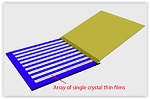
For fabrication of organic ferroelectric devices, one of the problems to be solved is to make a homogeneous thin film. The developed printing technique that stimulates thin-film formation from a solution allows formation of highly uniform single-crystalline thin films of organic ferroelectrics. The thin-film device fabricated by the developed technique worked as a memory device with only 3 V which is lower than operation voltage of various memory devices. The developed technique is expected to accelerate the research and development on low power consumption device of printed electronics such as ferroelectric memories and nonvolatile semiconductor FETs.
Details of the results will soon be published online in a German scientific journal, Advanced Materials.
Schematic of fabrication process of single-crystalline thin films of organic ferroelectric molecules
Social Background of Research
Active R&D of the "printed electronics", which applies printing technologies to the production of electronic devices by forming precise, high-quality, metallic and/or semiconducting patterns, has been conducted globally. So far, several printing methods have been enthusiastically developed to fabricate metallic wires and semiconductor layers for transistors, although the development of printing techniques for other types of materials has not been conducted enough. Ferroelectric materials could reduce the power consumption of electronic devices such as ferroelectric memories in IC cards and nonvolatile semiconductor FETs. Therefore, it is required to develop patterning techniques for ferroelectric thin films though printing technologies.
Ferroelectric materials are generally composed of inorganic materials so that it was considered to be difficult to apply a printing process. Although organic ferroelectric polymer materials are applicable to a printing process, their ferroelectric characteristics are inferior to those of inorganic materials. In recent years, research and development of organic ferroelectrics composed of small molecules have advanced. Some new organic materials showing superior characteristics comparable to inorganic ones have been found. Though thin-film formation of these materials is indispensable for making them into devices, it is difficult to form thin films of the materials. Therefore, it was desired to develop a fabrication technique of uniform thin film without any pinholes through a printing process.
Page 1 of 3
Share on:


Subscribe
Stay ahead of the technologies shaping the future of electronics with our latest newsletter, Advanced Electronics Packaging Digest. Get expert insights on advanced packaging, materials, and system-level innovation, delivered straight to your inbox.
Subscribe now to stay informed, competitive, and connected.
Suggested Items
MacDermid Alpha to Address Silver Price Volatility Solutions at ECTC 2026
05/15/2026 | MacDermid AlphaAs volatile silver prices continue to place pressure on semiconductor packaging costs and supply chain predictability, MacDermid Alpha Electronics Solutions will highlight material strategies that help manufacturers reduce dependence on silver without sacrificing reliability, thermal performance, or manufacturing efficiency.
Rethinking Reinforcement Materials for Advanced Packaging
05/14/2026 | Ivana Ivanovic, Flexiramics B.V.Materials that once quietly supported the industry are now becoming limiting factors. The electronics industry is experiencing unprecedented pressure as RF systems push into mmWave frequencies, high-speed digital architectures advance into their next performance generation, and power densities climb across automotive, telecom, aerospace, and computing. Reinforcement materials, long treated as a background detail in laminate design, are suddenly at the centre of performance, reliability, and supply‑chain discussions.
Rethinking Stackup, Materials, and Tolerances in Modern Designs
05/14/2026 | Kristin Moyer, Global Electronics AssociationThe simple rectangular rigid PCB is becoming increasingly infrequent. This reality necessitates designing with concepts well outside traditional rigid PCB methodologies. For example, the designer of wearable electronics may need to implement conductive fibers integrated into the textile material. Heads-up displays, like those in VR/AR headsets and glasses, require transparent circuitry etched into the display glass. The process of designing without a rule book usually starts with something other than the traditional board design process.
I-Connect007 Announces Upcoming Issue of Advanced Electronics Packaging Digest
05/13/2026 | I-Connect007The next issue of Advanced Electronics Packaging Digest examines the materials, architectures, and integration strategies shaping the next phase of electronics innovation, from reinforcement materials under thermal and frequency pressure to heterogeneous integration and advanced packaging as a system-level scaling factor.
Indium Experts to Address Data Center Thermal Management and Sintering Standards at SMTA Conference
05/13/2026 | Indium CorporationAs a leading materials provider for the advanced electronic packaging market, Indium Corporation® experts will share their technical insight and knowledge on two critical industry topics—data center thermal management and sintering protocols—at the SMTA Electronics in Harsh Environments Conference, May 19-21, in Amsterdam, Netherlands.