


 It’s Only Common Sense: Customers Capabilities—and Confidence
 Beyond the Board: How a Diminished Supplier Base Affects Complex PCB Manufacturing Readiness in Defense


MechSE Researchers Create One-step Graphene Patterning Method
April 28, 2016 | University of IllinoisEstimated reading time: 2 minutes
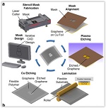
Researchers from the University of Illinois at Urbana-Champaign have developed a one-step, facile method to pattern graphene by using stencil mask and oxygen plasma reactive-ion etching, and subsequent polymer-free direct transfer to flexible substrates.
Graphene, a two-dimensional carbon allotrope, has received immense scientific and technological interest. Combining exceptional mechanical properties, superior carrier mobility, high thermal conductivity, hydrophobicity, and potentially low manufacturing cost, graphene provides a superior base material for next generation bioelectrical, electromechanical, optoelectronic, and thermal management applications.
“Significant progress has been made in the direct synthesis of large-area, uniform, high quality graphene films using chemical vapor deposition (CVD) with various precursors and catalyst substrates,” explained SungWoo Nam, an assistant professor of mechanical science and engineeringat Illinois. “However, to date, the infrastructure requirements on post-synthesis processing—patterning and transfer—for creating interconnects, transistor channels, or device terminals have slowed the implementation of graphene in a wider range of applications.”“In conjunction with the recent evolution of additive and subtractive manufacturing techniques such as 3D printing and computer numerical control milling, we developed a simple and scalable graphene patterning technique using a stencil mask fabricated via a laser cutter,” stated Keong Yong, a graduate student and first author of the paper, “Rapid Stencil Mask Fabrication Enabled One-Step Polymer-Free Graphene Patterning and Direct Transfer for Flexible Graphene Devices" appearing in Scientific Reports.
“Our approach to patterning graphene is based on a shadow mask technique that has been employed for contact metal deposition,” Yong added. “Not only are these stencil masks easily and rapidly manufactured for iterative rapid prototyping, they are also reusable, enabling cost-effective pattern replication. And since our approach involves neither a polymeric transfer layer nor organic solvents, we are able to obtain contamination-free graphene patterns directly on various flexible substrates.”Nam stated that this approach demonstrates a new possibility to overcome limitations imposed by existing post-synthesis processes to achieve graphene micro-patterning. Yong envisions this facile approach to graphene patterning sets forth transformative changes in “do It yourself” (DIY) graphene-based device development for broad applications including flexible circuits/devices and wearable electronics.
“This method allows rapid design iterations and pattern replications, and the polymer-free patterning technique promotes graphene of cleaner quality than other fabrication techniques,” Nam said. “We have shown that graphene can be patterned into varying geometrical shapes and sizes, and we have explored various substrates for the direct transfer of the patterned graphene.”
In addition to Nam and Yong, study co-authors include Ali Ashraf and Pilgyu Kang from the Department of Mechanical Science and Engineering at Illinois.
Share on:


Subscribe
Stay ahead of the technologies shaping the future of electronics with our latest newsletter, Advanced Electronics Packaging Digest. Get expert insights on advanced packaging, materials, and system-level innovation, delivered straight to your inbox.Subscribe now to stay informed, competitive, and connected.
Suggested Items
OE‑A Publishes 10th Edition of the Roadmap for Flexible and Printed Electronics
04/22/2026 | OE-AWith the publication of the 10th edition of the “OE-A Roadmap for Flexible and Printed Electronics,” the OE-A, an international working group for printed electronics within the VDMA, once again presents the central guidance and reference document for the industry.
Global Flexible PCB Market to Nearly Double, Reaching $41.7 Billion by 2030
04/03/2026 | Globe NewswireThe global flexible printed circuit board (FPCB) market is projected to grow from $21.5 billion in 2024 to $41.7 billion by 2030, reflecting a compound annual growth rate (CAGR) of 12.3%, according to a new report from BCC Research.
China’s Top 3 FPC Manufacturers 2026: Advancing Sustainable Flexible Electronics
03/25/2026 | EINPresswire.comThe global transition towards compact, lightweight, and durable electronic devices is accelerating demand for advanced Flexible Printed Circuits (FPCs).
SMT Renting: Redefining Equipment Investment
03/24/2026 | Marcy LaRont, I-Connect007SMT Renting, based in Copenhagen, is challenging the traditional machine-ownership model with a flexible, service-based approach. Business Manager Christian Thers discusses how rental options, “stop and swap” flexibility, and a new pay-per-placement model help electronics manufacturers reduce risk and adapt quickly in an unpredictable market.
Global Market for Flexible Manufacturing Systems Set to Surge to $22.2 Billion by 2030
03/02/2026 | GlobeNewswireAccording to the latest study from BCC Research, “Global Market for Flexible Manufacturing Systems” is expected to increase from $15.2 billion in 2025 to $22.2 billion by the end of 2030, at a compound annual growth rate (CAGR) of 7.9% from 2025 through 2030.