


 The Chemical Connection: Reducing Etch System Water Usage, Part 2
 It’s Only Common Sense: Nice Guys Really Can Finish First
 The Right Approach: I Hear the Train A Comin'
Shaping Atomically Thin Materials in Suspended Structures
June 14, 2016 | Tohoku UniversityEstimated reading time: 1 minute
Researchers at Tohoku University have realized wafer-scale and high yield synthesis of suspended graphene nanoribbons. The unique growth dynamic has been elucidated through comparing experiments, molecular dynamics simulations and theoretical calculations made with researchers from the University of Tokyo and Hokkaido University.
Adding a mechanical degree of freedom to the electrical and optical properties of atomically thin materials can provide an excellent platform to investigate various optoelectrical physics and devices with mechanical motion interaction. The large scale fabrication of such atomically thin materials with suspended structures, remains a challenge.
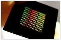
Led by Associate Prof. Toshiaki Kato, the team has used a bottom-up approach to demonstrate wafer-scale, high-yield synthesis of suspended graphene nanoribbon. This method has shed light on growth dynamics. It is possible to integrate over 1,000,000 suspended graphene nanoribbons in wafer-scale substrate with a high yield of over 90 %.
Suspended graphene nanoribbons in wafer-scale.
"Shaping atomically thin materials in suspended structures may provide a viable platform for nanoscale mechanical oscillators," says Kato.
Graphene nanoribbons are strips of graphene with quasi 1D structure (width ∼ a few tens nm, length, ∼ few µm). Different from 2D graphene, graphene nanoribbon includes band gap depending on its width and edge structures. It is expected to be utilized in next generation high performance optoelectrical semiconductor applications.
Kato adds, "The actualization of high yield and wafer-scale synthesis of suspended graphene nanoribbon will have an impact on the study of graphene nanoribbon, and be used in practical applications in a wide variety of fields."
Share on:


Suggested Items
LQDX Divests Aluminum Soldering Business - Mina™ - to Taiyo America Inc.
05/02/2024 | PRNewswireLQDX, formerly known as Averatek Corp., developer of high-performance materials for advanced semiconductor manufacturing, today announced that it has divested its aluminum soldering business – known as MinaTM – to Taiyo America Inc., a global market leader in advanced electronic materials.
Indium Corporation Expert to Present on Pb-Free Solder for Die-Attach in Discrete Power Applications
04/30/2024 | Indium CorporationIndium Corporation Product Manager – Semiconductor Dean Payne will present at the Advanced Packaging for Power Electronics conference, hosted by IMAPS, held May 8-9 in Woburn, Massachusetts, USA.
Real Time with... IPC APEX EXPO 2024: Adhesive Materials and Equipment Update with Dymax
05/01/2024 | Real Time with...IPC APEX EXPOVirginia Hogan, global business development manager at Dymax, discusses adhesive materials, dispensing and curing equipment, a new, high-reliability conformal coating, and various materials and dispensing methods.
Real Time with... IPC APEX EXPO 2024: Sustainability in the Industry
04/26/2024 | Real Time with...IPC APEX EXPOGuest Editor Henry Crandall and Chris Nash of Indium Corporation discuss the company's 90th anniversary and its focus on sustainability. They focus on the benefits of sustainable materials, their compatibility, and value propositions. The conversation also highlights how Durafuse LT technology's role in reducing reflow temperatures is leading to significant cost and energy savings. Nash also touches on downstream sustainability efforts such as using recycled materials for packaging.
SMC Korea 2024 to Highlight Semiconductor Materials Trends and Innovations on Industry’s Path to $1 Trillion
04/24/2024 | SEMIWith Korea a major consumer of semiconductor materials and advanced materials a key driver of innovation on the industry’s path to $1 trillion, industry leaders and experts will gather at SMC (Strategic Materials Conference) Korea 2024 on May 29 at the Suwon Convention Center in Gyeonggi-do, South Korea to provide insights into the latest materials developments and trends. Registration is open.