


 The Chemical Connection: Reducing Etch System Water Usage, Part 2
 It’s Only Common Sense: Nice Guys Really Can Finish First
 The Right Approach: I Hear the Train A Comin'
Gate-All-Around MOSFETs with Lateral Silicon Nanowires at Scaled Dimensions
June 20, 2016 | ImecEstimated reading time: 2 minutes
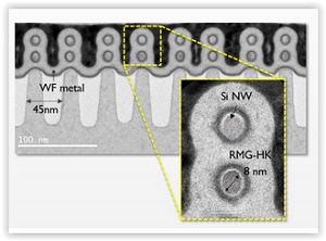
At the 2016 Symposia on VLSI Technology & Circuits, nano-electronics research center imec presented gate-all-around (GAA) n- and p-MOSFET devices made of vertically stacked horizontal silicon (Si) nanowires (NWs) with a diameter of only 8-nm. The devices, which were fabricated on bulk Si substrates using an industry-relevant replacement metal gate (RMG) process, have excellent short-channel characteristics (SS = 65 mV/dec, DIBL = 42 mV/V for LG = 24 nm) at performance levels comparable to finFET reference devices.
GAA devices architectures offer optimal electrostatic control, thereby enabling ultimate CMOS device scaling. In addition, horizontal NWs are a natural extension of RMG finFETs, in contrast to vertical NWs which require more disruptive technology changes. Furthermore, stacking of NWs maximizes the drive current per footprint. Imec successfully combined these three aspects, and, for the first time, demonstrated vertically stacked horizontal Si NWs at scaled dimensions: 8-nm-diameter wires, 45-nm lateral pitch, and 20-nm vertical separation.
Compared to the conventional bulk FinFET flow, imec implemented two major differences in the process flow. First, shallow trench isolation (STI) densification at 750°C resulted to preserve sharp silicon-germanium (SiGe)/Si interfaces, which is essential for well-controlled Si NW release. Second, a low-complexity ground plane doping scheme was applied, suppressing the bottom parasitic channel.
“By demonstrating stacked nanowires with solid electrostatic control, at scaled dimensions, and using an industry-relevant RMG process on bulk silicon substrates, imec has achieved breakthrough results that can pave the way to realizing sub-10nm technology nodes,” stated Dan Mocuta, Director Logic Device and Integration at imec. “The upcoming research phase will focus on achieving even denser pitches and on leveraging this knowledge to develop gate-all-around lateral nanowire CMOS devices.”
Imec’s research into advanced logic scaling is performed in cooperation with imec’s key partners in its core CMOS programs including GlobalFoundries, Intel, Micron, SK Hynix, Samsung, TSMC, Huawei, Qualcomm and Sony.
About imec
Imec performs world-leading research in nanoelectronics and photovoltaics. Imec leverages its scientific knowledge with the innovative power of its global partnerships in ICT, healthcare and energy. Imec delivers industry-relevant technology solutions. In a unique high-tech environment, its international top talent is committed to providing the building blocks for a better life in a sustainable society. Imec is headquartered in Leuven, Belgium, and has offices in Belgium, the Netherlands, Taiwan, USA, China, India and Japan. Its staff of about 2,500 people includes about 740 industrial residents and guest researchers. In 2015, imec's revenue (P&L) totaled 415 million euro.
Share on:


Suggested Items
IMI Welcomes New CEO
05/03/2024 | IMIIntegrated Micro-Electronics, Inc. (IMI),The IMI Board of Directors announced, in a disclosure dated April 25, 2024, the appointment of Louis Sylvester Hughes, Chief Executive Officer (CEO).
Gstar Announced the Strategic Move: Groundbreaking of Silicon Wafer Factory Construction in Indonesia
05/03/2024 | PRNewswireRecently, Gstar held a groundbreaking ceremony for its silicon rod and silicon wafer factory, marking the beginning of the rapid construction phase.
ZESTRON Academy Launches 2024 Advanced Packaging & Power Electronics Webinar Series
05/01/2024 | ZESTRONZESTRON, the leading global provider of high-precision cleaning products, services, and training solutions in the electronics manufacturing and semiconductor industries, proudly announces the launch of its highly anticipated webinar series on Advanced Packaging & Power Electronics, a webinar series on the latest innovations, cleaning, and corrosion challenges.
On the Line With… Talks With Cadence Expert on SI/PI for PCB Designers
05/02/2024 | I-Connect007In “PCB 3.0: A New Design Methodology—SI/PI for PCB Designers,” subject matter expert Brad Griffin, Cadence Design Systems, discusses how an intelligent system design methodology can move some signal and power integrity decision-making into the physical design space, offering real-time feedback.
The New Industry: Will the Growth Continue?
04/30/2024 | I-Connect007 Editorial TeamHow sustainable are the primary financial models in the United States regarding PCB fabrication shops? In this interview with economic experts Shawn DuBravac and Tom Kastner, we explore what’s happening with U.S. printed circuit board shops in today’s market, how consolidation affects the industry, and what can be done.