


 American Made Advocacy: What About the Rest of the Technology Stack?
 It’s Only Common Sense: Great Ideas From John Mitchell’s Book on Hiring Habits
 Punching Out: Breaking Out of the Valuation Box
Germs Add Ripples to Make 'Groovy' Graphene
July 12, 2016 | UICEstimated reading time: 3 minutes
Graphene, a two-dimensional wonder-material composed of a single layer of carbon atoms linked in a hexagonal chicken-wire pattern, has attracted intense interest for its phenomenal ability to conduct electricity. Now University of Illinois at Chicago researchers have used rod-shaped bacteria – precisely aligned in an electric field, then vacuum-shrunk under a graphene sheet – to introduce nanoscale ripples in the material, causing it to conduct electrons differently in perpendicular directions.
The resulting material, sort of a graphene nano-corduroy, can be applied to a silicon chip and may add to graphene’s almost limitless potential in electronics and nanotechnology. The finding is reported in the journal ACS Nano.
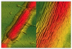
Atomic force microscopy image of a graphene sheet draped over a Bacillus bacterium (left). The bacterium is about 1 micron or 1/25,000 of an inch wide. After applying vacuum and heat treatment, regular wrinkles form in the graphene (right, at twice the magnification). — Photo: UNIVERSITY OF ILLINOIS AT CHICAGO/Vikas Berry
“The current across the graphene wrinkles is less than the current along them,” says Vikas Berry, associate professor and interim head of chemical engineering at UIC, who led the research.
The key to formation of these wrinkles, he said, is graphene’s extreme flexibility at the nanometer scale, which allows formation of carbon nanotubes.
“The wrinkle opens a ‘V’ in the electron cloud around each carbon atom,” Berry said, creating a dipole moment, which can open an electronic band gap that flat graphene does not have.
Other researchers have created wrinkles in graphene by stretching the sheet and letting it snap back. But such wrinkles are not confined in microscale and cannot be directed towards a location on a micro-device, Berry said.
He and his colleagues came up with a unique way to introduce circumscribed, guided, and regular graphene ripples using bacillus bacteria, by using the graphene itself as a check-valve to alter the volume of the cells.
The researchers placed the bacteria in an electric field, causing them to line up like strings of hot dogs in repeating rows. Then they applied a sheet of graphene over the top.
“Under vacuum, the graphene lifts, and lets water out,” Berry said. But under pressure, graphene sits back down on the substrate and prevents water from re-entering the bacteria, he said.
“It’s a nanoscopic valve that actuates unidirectional fluid flow in a microorganism,” Berry said. “Futuristically, this valve operation could be applied to microfluidic devices where we want flow in one direction but not the other.”
After the bacteria have been vacuum-shrunk, the graphene reconforms, but with wrinkles. After heat treatment, the resulting permanent ripples atop the bacteria are all aligned longitudinally, with a height of 7 to 10 nanometers, and a wavelength of about 32 nm.
The wrinkles were observed by field emission scanning electron microscopy, which must be done under high vacuum, and by atomic force microscopy at atmospheric pressure.
“The [ripple] wavelength is proportional to the thickness of the material, and graphene is the thinnest material in the world,” Berry said. “We envision that with graphene one could make the smallest wavelength wrinkles in the world – about 2 nanometers.”
The next goal, he said, will be to create processes to further refine the ripples and vary their amplitude, wavelength and longitudinal length.
To measure the effect of the ripples’ orientation on the carrier transport, graduate student Shikai Deng, the lead author of the paper, fabricated a plus-shaped device with bacteria aligned parallel to one pair of electrodes and perpendicular to another pair. He found the rippled graphene’s conduction barrier was greater in the transverse direction than in the longitudinal direction.
The introduction of oriented ripples to graphene represents an entirely new material, Berry said.
“Along with carbon nanotubes, graphene and fullerene, this is a new carbon allotrope – a half carbon nanotube linked to graphene,” he said. “The structure is different, and the fundamental electronic properties are new.”
The research was funded by the National Science Foundation and UIC.
In addition to Berry and Deng, co-authors on the ACS Nano study are Sanjay Behura of the UIC department of chemical engineering; Enlai Gao, Yanlei Wang and Zhiping Xu of Tsinghua University in Beijing; Soumyo Sen and Petr Král of the UIC department of chemistry; and T. S. Sreeprasad of Clemson University.
Share on:


Suggested Items
The Shaughnessy Report: Unlock Your High-speed Material Constraints
05/15/2024 | Andy Shaughnessy -- Column: The Shaughnessy ReportThe world of PCB materials used to be a fairly simple one. It was divided into two groups: the “traditional” laminates, often called FR-4, and the high-speed laminates developed especially for high-speed PCBs. These were two worlds that usually didn’t collide. But then traditional laminates started getting better, and high-speed designers and design engineers took notice and started to reconsider what FR-4 could be used for.
Breaking High-speed Material Constraints: Design007 Magazine — May 2024
05/14/2024 | I-Connect007 Editorial TeamDo you need specialty materials for your high-speed designs? Maybe not. Improvements in resins mean designers of high-speed boards can sometimes use traditional laminate systems instead of high-speed materials, saving time and money while streamlining the fab process. In the May 2024 issue of Design007 Magazine, our contributors explain how to avoid overconstraining your materials when working with high-speed boards.
Indium Experts to Present at Electronics in Harsh Environments SMTA Conference
05/13/2024 | Indium Corporationndium Corporation Technical Manager for Europe, Africa, and the Middle East, Karthik Vijay, will deliver a technical presentation and Indium Corporation Senior Technologist, Dr. Ronald Lasky, will deliver both a workshop and technical presentation at the Electronics in Harsh Environments SMTA Conference on May 14-16 in Copenhagen, Denmark.
Ansys’ Collaboration with Schrödinger will Accelerate Materials Development with Unprecedented Multiscale Simulation
05/09/2024 | ANSYSAnsys and Schrödinger are collaborating to deliver an ICME approach that bridges the gap between materials discovery and product development.
2024 Apple iPad Pro Estimated to Ship Between 4.5 to 5 Million Units
05/08/2024 | TrendForceApple’s recent product launch in May introduced a lineup of new tablets featuring advanced AMOLED screens. Notably, the Pro version boasts a dual-layer tandem structure designed to address the longstanding challenges of screen burn-in and lifespan that are common with AMOLED displays.