


 Knocking Down the Bone Pile: Precision Milling of Underfilled SMT Components
 Learning with Leo: Drones—Meeting Demand Without Compromise
 Nolan’s Notes: Our Spotlight on North America


Package-on-Package Warpage Characteristics and Requirements
July 25, 2016 | Wei Keat Loh, Intel Malaysia, and Haley Fu, iNEMIEstimated reading time: 3 minutes

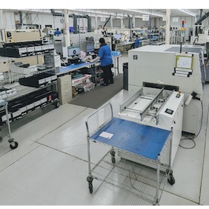
Electronics packaging technology has been relentlessly changing and pushing design boundaries, leading to adoption of new materials, assembly processes, ultra-small geometries, and 2.5D and 3D integration. These changes have driven multiple assembly and surface mount challenges, and among these are concerns about package warpage. Current qualification criteria and standards are not adequate to predict good yield results at first- and second-level assemblies. Furthermore, measurement methods (dimensional and test) are neither common nor up-to-date.
The International Electronics Manufacturing Initiative (iNEMI) organized the Warpage Characteristics of Organic Packages Project to identify primary factors that can contribute to the warpage performance of selected components during typical SMT processes. The project team's plan was to define a qualification method and a set of criteria (e.g., sample size, precondition, variations of material and processes at the first and second levels) that could be used to evaluate warpage characteristics of new and existing packages in the design and manufacture of products. Their objective was to better understand package warpage characteristics across different package types and attributes. The project has, to date, evaluated several types of packages. This article focuses on the work related to package-on-package (PoP).
PoP is widely used in mobile devices due to its integrated design, lower cost and faster time to market. Understanding warpage characteristics and requirements of this type of package is critical to ensuring that both the top and bottom package can be mounted with minimal yield lost. The current state of PoP warpage requirements has not been reevaluated and formed in clear specification other than customer-specific requirements. The typical SMT defect modes, such as non-wet open, solder bridging, head and pillow, and non-contact open (Figure 1) are applicable to both the joints between the PoP bottom package with the board and the PoP memory package. Other gross SMT defects can occur when there are geometry interferences between the PoP packages. This shows there is a need for ensuring that the warpage between PoP bottom and memory package is compatible. Efforts to leverage the warpage character-such behavior. Eslampour, lists many measurement tools that can be used to measure the dynamic warpage of a package. The most common tool made available for this study was the thermal shadow moiré tool. The ability to measure warpage at elevated temperature provides better risk assessment for the formation of component board assembly joints. The common convention used to define the warpage direction is based on "+" and "–" magnitude which represent convex and concave direction. However, there are shapes that are hard to determine just using these two signs.
Figure 1: Typical SMT defect modes.
The measurement was conducted based on the availability of the sample and perceived risk level. There were three preconditioning considerations: "as is," "bake" and "MET" (manufacturing exposure time), listed in Table 2. The purpose of these considerations is to mimic potential conditions prior to board assembly.
'As is' mimics the potential condition where packages are directly mounted to the board after taken out of sealed bags without much staging time. 'Bake' mimics the condition where the package is baked after being staged for unknown condition prior to board assembly. The baking process potentially alters the stress state of the package and removes any diffused moisture. MET nine days mimics the condition where the package is being staged in the factory floor for nine days, exposed to 30°C and 60%RH prior to component board assembly process. The typical MSL 3 calls for a maximum seven days of staging, but the work here extended to nine days to take into account any unforeseen circumstances.
These three precondition environments may potentially demonstrate different package warpage behavior and board assembly yield depending on the packaging technology used. Due to uneven samples acquired, some package types listed here were not subjected to all these preconditions.
To read this entire article, which appeared in the July 2016 issue of SMT Magazine, click here.
Share on:


Testimonial
"Our marketing partnership with I-Connect007 is already delivering. Just a day after our press release went live, we received a direct inquiry about our updated products!"
Rachael Temple - AlltematedSuggested Items
Indium Experts to Address Data Center Thermal Management and Sintering Standards at SMTA Conference
05/13/2026 | Indium CorporationAs a leading materials provider for the advanced electronic packaging market, Indium Corporation® experts will share their technical insight and knowledge on two critical industry topics—data center thermal management and sintering protocols—at the SMTA Electronics in Harsh Environments Conference, May 19-21, in Amsterdam, Netherlands.
KYZEN to Focus on Aqueous and Stencil Cleaning Solutions at SMTA Juarez Expo and Tech Forum
05/12/2026 | KYZENKYZEN, the global leader in innovative environmentally friendly cleaning chemistries, will exhibit at the SMTA Monterrey Expo & Tech Forum scheduled to take place on Thursday, May 21 at Injectronics Convention Center in Ciudad Juarez, Chihuahua.
Knocking Down the Bone Pile: Precision Milling of Underfilled SMT Components
05/13/2026 | Nash Bell -- Column: Knocking Down the Bone PileUnderfill is a polymeric material used to fill the gap between a printed circuit board and the underside of surface-mount area-array packages such as BGA, QFP, and QFN devices, thereby surrounding and protecting the solder interconnections. This material increases the component's reliability when subjected to mechanical impacts and shocks by distributing forces.
BGA Technology Expands Inspection Capabilities with Creative Electron TruView X-ray System
05/08/2026 | BGA TechnologyBGA Technology, a leading provider of advanced electronics testing and inspection services, has enhanced its inspection capabilities with the addition of a Creative Electron TruView™ Simplex X-ray system at its Holbrook, New York facility.
AQUANOX A4727 and A4625 Lead KYZEN Offerings at SMTA Oregon Expo and Tech Forum
05/06/2026 | KYZENKYZEN, the global leader in innovative environmentally responsible cleaning chemistries, will exhibit at the SMTA Oregon Expo and Tech Forum scheduled to take place Thursday, May 19 at the Wingspan Event and Conference Center in Hillsboro, Oregon.