


 Trouble in Your Tank: Understanding Interconnect Defects, Part 1
 It’s Only Common Sense: Marketing Isn’t Fluff, It’s Ammunition
 Driving Innovation: Mechanical and Optical Processes During Rigid-flex Production


Nano Dimension Supplies First DragonFly 2020 System
August 25, 2016 | Nano DimensionEstimated reading time: 1 minute
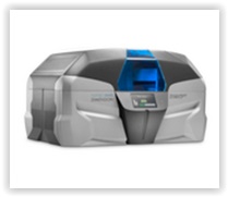
Nano Dimension Ltd. announced today that its wholly owned subsidiary, Nano Dimension Technologies, has supplied the first DragonFly 2020 system designated for 3D circuitry and PCBs. The supply was made to a leading defense company in Israel for evaluation purposes and is expected to be installed at the partner's site in the coming days.
To date, Nano Dimension has proven its capabilities of printing multilayer electric circuits in lab conditions. With the first supply of the DragonFly 2020 system for testing, Nano Dimension marks yet another breakthrough for the company. This is the first key step towards the potential commercialization of Nano Dimension's products.
"We are proud to have reached this important milestone," said Amit Dror, CEO of Nano Dimension. "Supplying our first system to a beta partner is a tremendous achievement for Nano Dimension and the electronic industry. Nano Dimension set an ambitious goal to develop a revolutionary product that – until now- did not exist in the market, based on advanced technology that combines hardware, nano-chemistry and software. Today, only two years since our first fundraising and since our shares began trading on the TASE, we mark this important milestone of supplying our first system to a beta partner, enabling them to print multilayer electric circuits in several hours. We look forward to completing production of more printers destined for additional partners and customers in Israel and around the world."
About Nano Dimension Ltd.
Nano Dimension, founded in 2012, focuses on development of advanced 3D printed electronics systems and advanced additive manufacturing. Nano Dimension's unique products combine three advanced technologies: 3D inkjet, 3D software and nanomaterials. The company's primary products include the first 3D printer dedicated to printing multi-layer PCBs (printed circuit boards) and advanced nanotechnology-based conductive and dielectric inks.
In addition to the trading of the company's American Depositary Shares on NASDAQ, the company's ordinary shares are also traded on the TASE in Israel. The Bank of New York Mellon serves as the depositary for Nano Dimension.
Share on:


Testimonial
"Advertising in PCB007 Magazine has been a great way to showcase our bare board testers to the right audience. The I-Connect007 team makes the process smooth and professional. We’re proud to be featured in such a trusted publication."
Klaus Koziol - atgSuggested Items
UHDI Fundamentals: UHDI Technology and Automated Inspection
11/03/2025 | Anaya Vardya, American Standard CircuitsFollowing up on the last article on integrating ultra high density interconnect (UHDI) PCB technologies and Quality 5.0, here we will do a deeper dive into the automated inspection component. UHDI applications demand extreme precision, with line/space dimensions below 25 µm and microvias below 30 µm. Automated inspection systems are essential to achieving the defect-free fabrication required at these scales, and legacy automated inspection systems are becoming obsolete and ineffective.
OSI Systems Reports Fiscal Q1 2026 Financial Results
10/31/2025 | BUSINESS WIREOSI Systems, Inc. announced its financial results for the first quarter of fiscal 2026.
Aircraft Wire and Cable Market to surpass USD 3.2 Billion by 2034
10/30/2025 | Global Market Insights Inc.The global aircraft wire and cable market was valued at USD 1.8 billion in 2024 and is estimated to grow at a CAGR of 5.9% to reach USD 3.2 billion by 2034, according to recent report by Global Market Insights Inc.
David Schild Addresses Printed Circuit Board Issues as a Panelist at AUVSI
10/30/2025 | PCBAAOn October 28, Printed Circuit Board Association of America executive director David Schild appeared on a panel at the Association for Uncrewed Vehicle Systems International (AUVSI) conference on the topic of “First Supply Chains: Strengthening the Industrial Base for Autonomy.” PCBAA sponsored the event and Schild shared his views on issues facing the American microelectronics industry.
Real Time with... SMTAI 2025: Koh Young's Innovations in SMT Inspection Technology
10/30/2025 | Real Time with...SMTAIJoel Scutchfield discusses his background as well as Koh Young's advancements in inspection technology. The conversation covers various inspection systems, including the flagship Zenith 2 system and recent software upgrades.