


 Material Insight: The Dielectric Constant of PCB Materials
 American Made Advocacy: What About the Rest of the Technology Stack?
 It’s Only Common Sense: Great Ideas From John Mitchell’s Book on Hiring Habits
Notre Dame Researchers Find Transition Point in Semiconductor Nanomaterials
September 6, 2016 | Notre DameEstimated reading time: 2 minutes
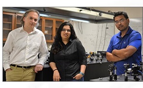
Collaborative research at Notre Dame has demonstrated that electronic interactions play a significant role in the dimensional crossover of semiconductor nanomaterials. The laboratory of Masaru Kuno, professor of chemistry and biochemistry, and the condensed matter theory group of Boldizsár Jankó, professor of physics, have now shown that a critical length scale marks the transition between a zero-dimensional, quantum dot and a one-dimensional nanowire.
The findings, "Dimensional crossover in semiconductor nanostructures," were published in Nature Communications. Matthew P. McDonald and Rusha Chatterjee of Kuno's laboratory and Jixin Si of Jankó's group are also authors of the publication.
A quantum dot structure possesses the same physical dimensions in every direction while a quantum wire exhibits one dimension longer than the others. This means that quantum dots and nanowires made of the same material exhibit different optical and electrical responses at the nanoscale since these properties are exquisitely size- and shape-dependent. Understanding the size- and shape-dependent evolution of nanomaterial properties has therefore been a central focus of nanoscience over the last two decades. However, it has never been definitively established how a quantum dot evolves into a nanowire as its aspect ratio is made progressively larger. Do quantum properties evolve gradually or do they suddenly transition?
Kuno's laboratory discovered that a critical length exists where a quantum dot becomes nanowire-like. The researchers achieved this breakthrough by conducting the first direct, single particle absorption measurements on individual semiconductor nanorods, an intermediate species between quantum dots and nanowires. Single particle rather than ensemble measurements were used to avoid the effects of sample inhomogeneities. Furthermore, an absorption approach rather than an often-used emission approach was employed to circumvent existing limitations of modern emission-based single particle microscopy-namely, its restriction to the observation of highly fluorescent specimens.
The discovery marks a significant advance in our understanding of the size- and shape-dependent quantum mechanical response of semiconductor nanostructures. "All of the introductory-level solid state or semiconductor textbooks need to revise what they say about dimensional crossover," Jankó said. "This is another example where interactions makes things completely different." Beyond this, Kuno suggests that the single particle absorption approach advanced in the study "has practical, real-world applications, maybe 40 years down the road." Examples include the generic and label-free ultrasensitive detection of chemical and biomolecular species of paramount interest within the spheres of homeland security as well public health.
Kuno's group performed the experiments that led to the discovery while Jankó's group provided theoretical support.
Share on:


Suggested Items
Kimball Electronics Thailand Helps Save Lives by Hosting a Blood Drive
05/14/2024 | Kimball ElectronicsKimball Electronics Thailand employees took part in a blood donation event. The blood drive took place in the Rajapruek Building at Laem Chabang Industrial Estate Office.
SEMI Applauds U.S. CHIPS Act Award for Polar Semiconductor Facility in Minnesota
05/14/2024 | SEMISEMI, the industry association serving the global semiconductor and electronics design and manufacturing supply chain, applauded the United States Department of Commerce’s announcement of a Preliminary Memorandum of Terms for an award under the CHIPS and Science Act to support the expansion and modernization of Polar Semiconductor’s fab in Minnesota.
Punching Out: Breaking Out of the Valuation Box
05/09/2024 | Tom Kastner -- Column: Punching Out!Most companies are in a “valuation box.” That is, the value of the company, based on a market multiple, is not equal to the value of the assets. Or worse, once debt is paid off, the net proceeds would actually be negative. Here are some tips for getting out of the box.
IDC Forecasts Slower Growth for Global Telecommunications Services Market: Could AI Help Telcos to Maintain Healthy Margins?
05/08/2024 | IDCWorldwide spending on Telecom Services and Pay TV Services reached $1,509 billion in 2023, an increase of 2.1% over 2022, according to the International Data Corporation (IDC) Worldwide Semiannual Telecom Services Tracker.
Q1 Global Semiconductor Sales Increase 15.2% YoY
05/07/2024 | SIAThe Semiconductor Industry Association (SIA) announced worldwide sales of semiconductors totaled $137.7 billion during the first quarter of 2024, an increase of 15.2% compared to the first quarter of 2023 but 5.7% less than the fourth quarter of 2023.